




X-Ray Inspection of Ball Grid Array Solder Joints
Posted by Nash Bell on Jul 28th 2026
Advantages of BGA Devices
Ball grid array (BGA) devices are omnipresent throughout electronic products primarily due to numerous advantages including compact packaging, a durable format relative to leaded devices, and improved performance because of shorter signal paths.
BGAs provide improved electrical performance due to short connections between the internal silicon die and the PCB board reducing inductance and capacitance leading to superior signal integrity and faster operation speeds. BGAs also offer superior thermal performance since they allow heat to dissipate more effectively reducing the risk of overheating.
BGAs provide high density interconnection since unlike perimeter only packages such as quad flat pack (QFP) devices, BGAs utilizes the entire bottom surface of the device allowing for a much higher number of I/O connections in a smaller footprint. However, since solder interconnections of a BGA are hidden underneath the device this makes inspection of solder joints a challenging task.
Solder Joint Inspection Methods
A major advantage during the printed circuit assembly process is the ability of BGAs to self-align during reflow soldering as surface tension of the molten solder balls helps align the component to the PCB pads. Several methods can be used to inspect BGAs after solder reflow onto a printed circuit board including visual inspection, endoscope inspection, and X-ray inspection.
- Visual Inspection: Used with an optical microscope to view the outer rows of a BGA for wetting and ball to pad alignment.
- Endoscope Inspection: Used to view some inner rows of a BGA for wetting and alignment otherwise inaccessible by an optical microscope.
- X-ray Inspection: Used to inspect internal solder joints, detect voids within solder balls and identify bridging between solder balls that cannot be seen visually.
- Electrical Testing: Functional testing to ensure BGA connectivity but requires specialized equipment and skilled technicians and is a time-consuming process.
While optical microscope and endoscope forms of visual inspection are useful as an initial check of a BGA assembly, they are limited in the ability to detect other critical parameters such as voiding and solder bridging.
Acceptance Criteria
The key acceptance criteria for BGA assembly per the IPC-A-610 and J-STD-001 standards include:
- Alignment: Solder balls are centered and show no offset of the ball to land centers or spacing violations.
- Solder ball spacing: Solder balls do not violate minimum electrical clearance
- Solder connections: BGA solder balls contact and wet to the land forming a continuous elliptical round connection. No solder bridging, opens, missing balls, or unsoldered connections.
- Solder ball uniformity: While not considered a defect, solder balls that are not uniform in size, shape, coloration, and color contrast are considered a process indicator for class 2 and class 3.
- Solder voids: 30% or less of any ball in the X-ray image area.
- Solder ball appearance: Solder balls should show evidence of proper reflow, wetting and uniform collapse across the array.
- Head-in-Pillow: No head-in-pillow defects.
- Foreign object debris (FOD): No signs of conductive or loose debris that violates clearance or can affect function under or around BGA.
Popcorning
The term ‘popcorning’ is used to define a failure mode associated with moisture ingress to surface mount components such as BGAs. If moisture sensitive devices including BGAs are not retained in a nitrogen dry storage cabinet, they are susceptible to the popcorning phenomena. Popcorning occurs when a small amount of moisture trapped within the polymer molding of a BGA is converted into a large volume of steam during the solder reflow process. This causes the BGA package to expand like a kernel of cooked popcorn and can result in cracks within the BGA package which can lead to potential field failures.
Popcorning of BGAs can be indicated by the presence of bridging between adjacent solder balls underneath the device since the bottom of a BGA device is where it is thinnest. This results when the expansion of the package occurs during solder reflow causes it to ‘dish’ downward where the underneath of the package deforms and presses down on the solder balls. As the solder is liquidous at the time, it allows the solder from adjacent balls to coalesce and therefore produce solder bridging underneath the BGA device.
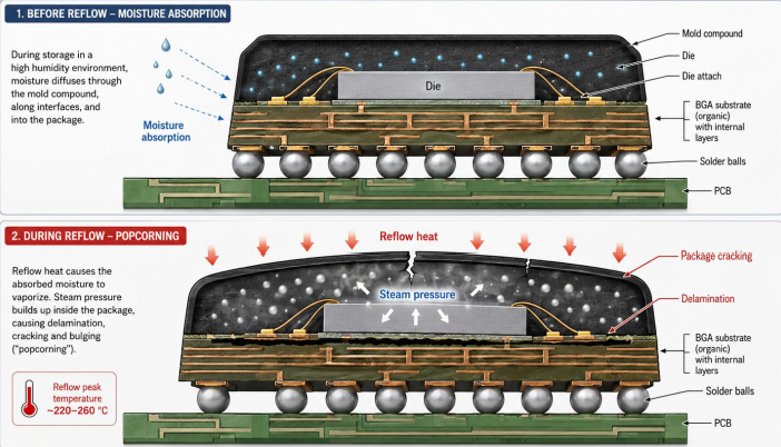
The most typical cause of popcorning is the hygroscopic sensitivity of the molding compound used to protect the die. Device manufacturers have been aware of package moisture sensitivity levels (MSL) for many years and have procedures in place to treat components prior to their use in the reflow process. With the move to lead-free solders that have substantially higher reflow temperatures, it makes BGA packages more susceptible to the threat of popcorning. This is due to the peak temperature that a BGA will be exposed to with lead-free alloys being approximately 20°C higher than tin-lead solders. As a result, it is suggested that a typical MSL will increase between one and three levels for the same device when used in a lead-free process.
Common Causes for Rejection
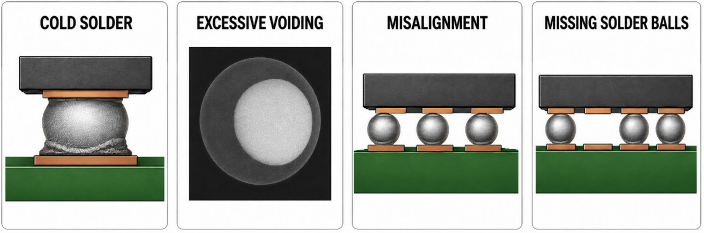
There are several anomalies that can occur during the assembly of a printed circuit board containing BGA devices. The most common are incomplete solder melting, excessive voids, a misaligned device, or missing solder balls.
- Partial Reflow or Cold Solder: Incomplete melting of solder balls during the solder reflow process resulting from inadequate time-temperature profile or insufficient dwell time.
- Excessive Voids: Large or clustered excessive voids within solder balls greater than 25%. Alternatively, this voiding requirement can be as low as 10% for mission critical applications such as aerospace, defense and medical products, etc.
- Misaligned or Shifted BGA: Device package shifted partially off PCB pads during reflow greater than the 25% allowable requirement.
- Missing or Broken Balls: Missing or damaged solder balls prior to placement
X-ray Inspection
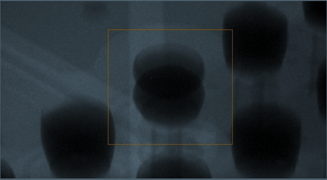
Transmissive, real-time X-ray using a tilt function should be used to document several potential defects during BGA inspection. Solder bridges are the most common defect which can be detected by this technique. Gross voids can be seen at greater power and magnification levels.
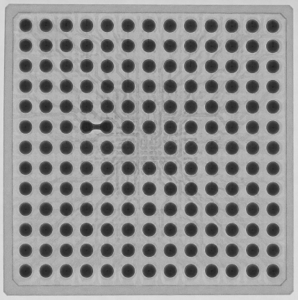
Defects such as opens and voids can be sometimes difficult to discern even with high-quality X-ray equipment. Inspection technicians need to be adequately trained in interpreting X-ray images to identify all types of defect conditions.
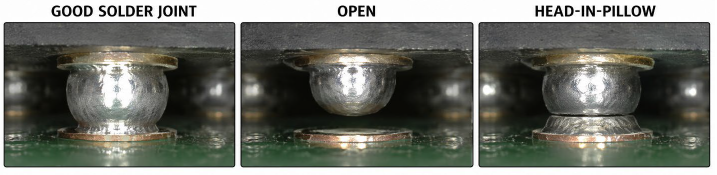
In addition, the concentricity, pitch, circularity, and solder ball diameter can also be measured as part of the BGA inspection process. With the proper equipment which either tilts the sample or the detector, even head-in-pillow defects can be noted.
Endoscopic inspection is a valuable supplemental tool for BGA inspection because it allows inspectors to view beneath the ball grid array and assess visible solder-joint surfaces that may not be fully characterized by X-ray alone. It can help determine whether reflow produced an acceptable
joint condition or signs of defects by revealing surface characteristics such as texture, uniformity, smoothness, color, brightness, wetting, and possible micro-cracking. Endoscopes also provide useful documentation through captured images and video, supporting inspection findings, customer review, process improvement, and failure analysis.
Conclusion
Effective BGA inspection requires more than just the right equipment, including X-ray capability. It also depends on accurate interpretation of inspection criteria and standards by trained, experienced inspectors. The ability to rework and inspect hundreds of BGA types across a wide range of board designs—using both industry-standard and customer-specific acceptance criteria—is essential. A robust BGA inspection protocol should therefore combine proven X-ray inspection expertise with the latest X-ray tools and techniques to reliably identify the full range of potential BGA defects.
It is also important to avoid excessive X-ray exposure during inspection, particularly when working with commercial off-the-shelf semiconductor devices, where radiation effects may be a concern. Methods for minimizing the impact of X-ray radiation will be discussed in a future column.
Written by Nash Bell, President of BEST Inc