




Salvaging Electronic Components: A Reliable Method for Reducing Electronic Waste, and Ensuring Economic Reuse
Posted by Nash Bell on Jul 28th 2026
By Nash Bell, President, BEST Inc.
The economic and environmental implications of electronic component salvage and reuse are
becoming increasingly significant with respect to the rising costs of semiconductor fabrication and
sustainability concerns. By extending the lifecycle of electronic components, salvaging, and
reconditioning of high-value devices contributes to a more sustainable electronics industry
enabling far-reaching and beneficial environmental goals.
Abstract
Component salvaging is the process of harvesting high-value electronic components from printed
circuit boards after removal from obsolete or superseded electronic products for reuse in new
electronic assemblies. This process reduces the environmental impact of electronic waste and
minimizes the reliance on energy intensive fabrication of new electronic components such as
complex and costly semiconductor devices.
Key Terms: Electronic waste, electronic recycling, rare earth elements, component reclamation,
sustainability, circularity, environmental impact, semiconductor manufacturing resources
Impact of Electronic Waste
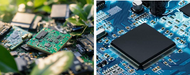
Electronic waste is becoming an increasing global issue at an alarming rate. Estimates are that by
2030 the world is on track to generate approximately eighty-two million tons of electronic waste per
year (see Figure 1a). Rapid technological advances, shorter product lifecycles, and supply chain
disruptions often lead manufacturers to create a bloated inventory of electronic products.
Unfortunately, some of this inventory ends up as electronic waste as components become
obsolete or surplus to forecasted requirements including high-value devices (see Figure 1b).
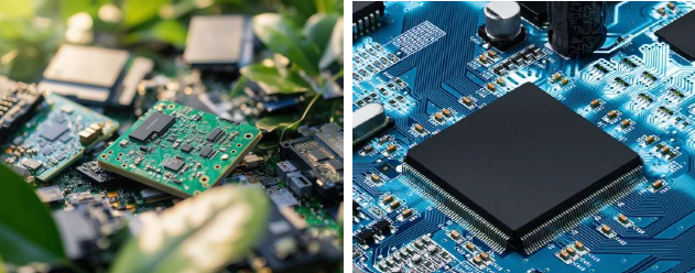
Fig. 1a) Example of discarded electronic waste (left), and 1b) high-value quad flat pack device (right)
Basic recycling practices have been employed to recapture valuable metals from electronic
components such as gold and other high value metals. For example, estimates are that four
thousand tons of electronic waste can generate up to 450 Kg (kilograms), or approximately 1,000
lbs. of recycled gold.
Rare Earth Elements
Many electronic components contain various rare earth elements (REE) utilized for their unique
electrochemical, magnetic, or luminescent properties. The problem is these REE elements are a
finite resource extracted from deposits within the earth. Unlike fossil fuels REE elements are
critical to emerging green technologies that enable a more sustainable future. Yet quantities of
REEs are lost daily in the form of discarded electronic components. The most common REE
elements used in electronic components include lanthanum (La), cerium (Ce), neodymium (Nd),
europium (Er), terbium (Tb), and dysprosium (Dy).
Rare earth elements are not rare but are common within many of the earth’s locations, what makes
these elements rare is the refining process that extracts them from the various ore deposits. Few
nations account for the majority of REEs with China accounting for approximately 70% of the total
global REE ore extraction. China’s dominance has emerged because it is willing to bear the
environmental costs of extraction and refining. Rare earth refinery facilities typically produce thick
smoke, huge piles of tailings consisting of toxic, metallic by-products often lying on the bare
ground typically exposed to rainwater runoff resulting in topsoil and groundwater pollution.
Pros and Cons of Electronic Recycling
Of the millions of tons of electronic waste that are discarded globally each year, less than 20% of
the raw materials and electronic components inside these devices are recycled. Consumer
electronics is a numbers game as many manufacturers compete for market share as most
companies may not have any economic incentive to build more durable devices that can last
longer before they need to be replaced. Additionally, most companies and consumers are not reusing
these devices or the components inside at the end of their lifespan. This is mainly due to the
difficulties of repairing these products, replacing obsolete components, or upgrading the software
without overtaxing the hardware. While the business of recovering precious metals and other
valuable materials from electronic waste is increasing, there are limits to recycling. In most cases
the printed circuit board and other devalued components are dumped into landfills or incinerated.
Extracting and recapturing valuable metals from recycled electronic components requires
advanced recycling practices such as bioleaching, utilizing micro-organisms, hydrometallurgy with
chemical leaching, or pyrometallurgy (smelting) at elevated temperature.
One major challenge in electronic waste recycling is the small size of components, which makes
isolating and extracting specific materials difficult. Not to mention the size of modern electronics,
such as smartphones, which often have printed circuit boards (PCBs) packed into tight and
sometimes difficult-to-access spaces. Recycling is currently one of the best methods to isolate
valuable metals and specific REEs from electronic waste, recouping value and preventing the need
for virgin resource extraction. Common practices such as hydrometallurgy do not require
considerable amounts of energy to pull off valuable metals in most cases.
The financial benefits of recycling should not be overlooked. The collection and processing of
electronic waste create jobs and can positively contribute to the economy. At the same time,
discarded electronics are kept out of landfills, where they pollute the environment in various ways.
Now for the bad news… while recycling is certainly more sustainable than disposing of electronic
waste, it is not without its flaws compared to other electronic waste solutions. Each electronic
waste recycling technique is unique with its own positives and negatives. Although pyrometallurgy
extraction (smelting) effectively extracts certain metals, it usually requires extreme temperatures
and may release greenhouse gases, metal vapors, and other toxic dioxins and furans during the
process depending on the method. Hydrometallurgy may not need as much energy, but common
practices generate hazardous chemical waste. Bioleaching is a very promising alternative.
However, as it stands, this approach may be slower and less scalable. Recycling is a reactive
approach to managing electronic waste. A more effective strategy for prevention is reducing waste
at the source through redistribution and designing products with circularity in mind.
Sustainability and Circularity
Electronic waste often contains hazardous materials that pose risks to human health and the
overall environment. Many of these toxins include mercury, lead, and brominated flame retardants
(BFRs). A circular supply chain is a strategy for keeping these materials from being dumped into
landfills together with electronic waste.
A circular economy closes resource loops and maximizes the lifetime value of materials. To
achieve this, electronic manufacturers follow a take, make, use, repair, repurpose, redistribute,
and then recycle model, whereas a linear economy follows a take, make, and dispose
methodology. Recycling is part of circularity however, the goal is to ensure that devices can be
utilized by another manufacturer, preventing this need for as long as possible.
Another consideration in a circular supply chain is designing products that are easier and
financially viable to repair and upgrade. Modular product design is a crucial aspect of promoting
circularity. Designing products that are easy to repair and encouraging buy-back schemes also
empower end-consumers to make more sustainable choices with their electronics purchases.
Being able to repair devices easily encourages people to fix what they own instead of replacing
them without thought.
Circularity prevents waste beyond just reducing discarded components. Many legacy components
(parts older than 10 years) may not be available via franchised distribution. Sometimes, one legacy
chip may prevent the scrap out of a large, old industrial piece of equipment, instead enabling a
successful and cost-effective repair.
Semiconductor Manufacturing Resources
A typical semiconductor fabrication plant (see Figure 2a and Figure 2b) requires millions of gallons
of ultra-purified water each day and a large volume of energy to operate. As an example, it is
projected that TSMC (Tiawan Semiconductor Manufacturing Company), one of the world’s largest
semiconductor manufacturers, will consume 12.5% of Taiwan’s total electricity in 2026. TSMC has stated it is their goal to strive toward having 60% of its energy to come from renewable sources by 2030 and 100% by 2040.
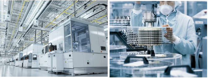
Fig. 2a) Typical semiconductor fabrication plant (left), and 2b) semiconductor fabrication processing (right)
The economic and environmental benefits of using salvaged electronic components in lieu of newly
fabricated semiconductor devices can be substantial and include several factors. In addition to
reducing electronic waste, salvaged and reconditioned high-value components provides
substantial energy savings. According to industry estimates it is estimated to take approximately
1,500 to 2,500 kWh (kilo watt hours) of energy to produce a single 300 mm-diameter
semiconductor wafer (see Figure 3a).
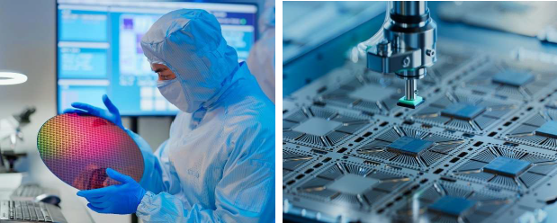
Fig. 3a) Inspection of 300 mm semiconductor wafer (left), and 3b) chip attachment to lead frames (right)
On average a single wafer yields approximately five hundred (500) chips (see Figure 3b), therefore
the energy required per individual chip is approximately 5 kWh. However, this figure can vary
depending on the semiconductor fabrication process and the size and complexity of each chip.
This estimate is solely for fabrication and does not include other factors such as the energy
required for extraction of raw materials, transportation, distribution, or device packaging.
Component Salvaging and Reclamation
When harvesting electronic components from printed circuit boards several factors need to be
considered. These include the type and level of physical damage to the component, the
components electro-static discharge (ESD) level, electrical overstress (EOS), moisture sensitivity
device (MSD) level, and the environmental conditions it has interacted with, together with other
factors. Outsourcing of the component salvaging process allows you to hire professionals who can
effectively take care of these critical factors and use high-performance tools and process
capability to successfully locate, remove, and procure valuable components from discarded
electronic products.
When selecting an outsource partner several factors should be evaluated to ensure the integrity
and quality of the component reclamation process. It is recommended to audit the outsource
partner to verify they have effective MSD processes in alignment with J-STD-033 guidelines. It is
also recommended that the outsource partner have numerous years of experience with BGA
salvaging and follows all applicable MSD, EOS, and ESD safeguards.
Pre-Baking
Baking printed circuit board assemblies prior to component removal is a critical step in preventing
moisture-related damage. Over time, moisture can become trapped in sensitive devices, and if this
moisture vaporizes during desoldering or reflow, it can cause internal cracking, delamination, or
the phenomenon known as “popcorning.” Pre-baking drives out this moisture, preserving the
functional integrity of components and ensuring compliance with J-STD-033 moisture mitigation
standards.
Component Removal
After mechanical disassembly, most components can be recovered using hot air or infrared (IR)
rework systems. Hot air systems deliver a controlled stream of heated air to raise both the
component and the surrounding printed circuit board to solder reflow temperature. Operators
must carefully manage airflow, temperature, and dwell time to prevent thermal damage or PCB
warping. Preheating the board before component removal is an effective practice that further
reduces thermal shock and helps preserve component integrity.
Infrared systems, in contrast, radiate heat directly into the component, minimizing thermal
exposure to nearby devices. The technique is highly dependent on variables such as component
color, reflectivity, and board material, making precise calibration and profiling essential.
Regardless of the method used, adherence to MSD handling procedures per J-STD-033 is crucial to
prevent component failure during removal, and thermal profiling ensures heating remains within
manufacturer-recommended specifications (see Table 1).
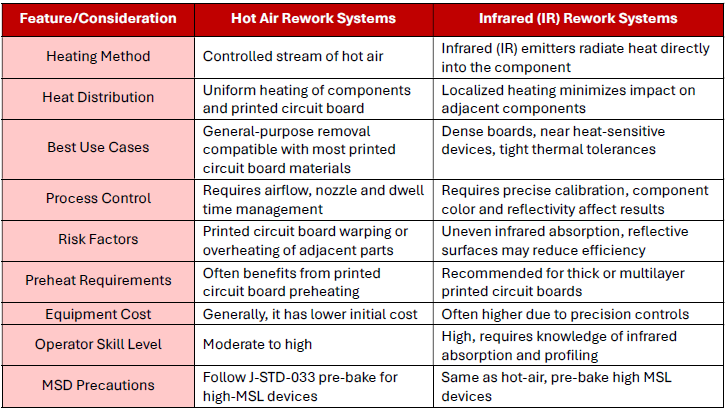
Table 1) Considerations for selecting electronic component salvaging systems.
Following mechanical disassembly most electronic components can be harvested for reuse in
future electronic products. Removal of electronic components from a printed circuit board can be
performed with either hot-air or infrared rework systems. Hot-air systems utilize a stream of hot-air
to uniformly heat the component, often a BGA device, as well as the PCB, enabling solder melting
and package removal (see Figure 4a). While effective this method requires careful management to
prevent potential thermal damage to adjacent components. Alternatively infrared systems employ
IR emitters to directly target the desired component or BGA, minimizing thermal impact on
surrounding areas and adjacent components. Calibration of infrared systems is crucial for
achieving uniform heating of the printed circuit board assembly.
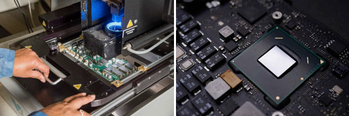
Fig. 4a) BGA removal with hot-air system (left), and 4b) salvaged BGA mounted on new PCB assembly (right)
Specialized tools and equipment are required to reliably remove and salvage electronic
components from printed circuit boards. These include high-quality professional soldering irons,
hot-air or infrared component removal systems, robotic hot solder dip machines, inspection
systems, stereo microscopes, cleaning systems, baking ovens, and various types of hand tools.
Operators performing component salvaging must be highly trained in the proper knowledge, skills
and protocols of MSD and ESD safeguards to ensure components are not damaged during the
removal, desoldering and reclamation process.
Electronic component salvaging includes reclamation of various types, of primarily surface mount
devices including ball grid array, land grid array and quad flat no-lead components which can be
salvaged and reconditioned for use in assembly of other circuit boards. The harvesting of electronic
components from printed circuit boards helps alleviate supply chain shortages of high-value or
hard-to-source electronic devices. Following reconditioning salvaged components are typically
laser marked for traceability and packaging on tape and reel per EIA-481 standards or in trays for
automated circuit board assembly (see Figure 4b).
Component Reconditioning
After removal from a printed circuit board the component leads and pads must be reconditioned to
remove any excessive or insufficient solder to prepare harvested components for future assembly.
Manual soldering can be used or robotic hot solder dip (RHSD) processing which involves removing
old solder balls from a BGA device and replacing them with new solder balls of a different alloy,
and/or restoring electrical integrity. While cost-effective, the RHSD method requires specialized
equipment and skilled technicians.
The first step in the BGA reballing process involves removing the original solder balls to expose the
interposer pads. BGA deballing can be accomplished manually or robotically. Manual deballing is
performed by wicking the solder balls using a soldering iron and copper braid. While this is an
effective and commonly used method, there is potential risk of damaging pads if not performed
properly. Robotic deballing is performed using a robotic hot solder dip (RHSD) machine (see Figure
5a and Figure 5b). Since robotic deballing is touch-free, the risk of scratching pads is significantly
reduced, however due to the extreme temperature of the molten solder wave, this process may
result in defects such as lifted pads if not controlled properly.
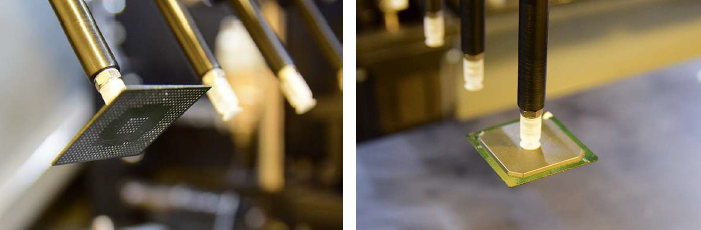
Fig. 5a) Ball grid device before automatic de-balling (left), and 5b) ball grid array being de-balled (right)
Once the solder balls have been successfully removed from a BGA, the next step is to attach new
spheres to the component, for which various methods are available. A common ball placement
method involves applying tacky flux to the component and using a fixture that matches the
component’s array (see Figure 6a). The fixture ensures proper ball alignment, while the flux helps
secure the balls in place for reflow. Alternatively fixture-less laser reballing can be used for finepitch
BGA devices of 0.4mm or less (see Figure 6b).
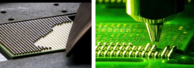
Fig. 6a) BGA reballing via custom fixture (left), and 6b) fixture-less 0.4 mm pitch laser reballing (right)
Following the reballing processes, inspection should be performed including verifying device
coplanarity, Z-height measurement of solder balls, missing solder balls, solder ball volume, shorts
between adjacent solder balls, and detection of any foreign object debris. A reliable reballing
processing is a vital step to ensuring high quality harvesting of BGA devices. The integrity of
reconditioned devices should be assured using endoscopic or X-ray inspection of the
interconnections (see Figure 7a and Figure 7b). Additional testing is optional and may include
solderability testing per J-STD-002 requirements. All reconditioned components should be cleaned
in a batch or in-line cleaning system with the appropriate solvent or aqueous cleaning agent to
remove all residual flux residues. After the cleaning process reconditioned electronic devices
should undergo bake out per J-STD-003 guidelines.
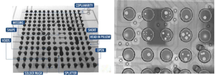
Fig. 7a) Defects visible via X-ray inspection (left), and 7b) solder voids evident in enlarged field-of-view (right)
Associated Risks
Re-using salvaged components from previously assembled printed circuit boards carries inherent
risks that can compromise both the reliability and safety of the final assembly. Components
removed from old or discarded boards may have been subjected to electrical overstress, excessive
thermal cycling, environmental contamination, or mechanical damage during prior service life.
Even if the component appears physically intact, unseen degradation - such as microcracks in
solder terminations, weakened leads, or subtle shifts in electrical characteristics - can lead to
early failure in the new product.
There are several testing options that can be utilized to reduce the risks associated with re-use of
salvaged electronic components (see Table 2).
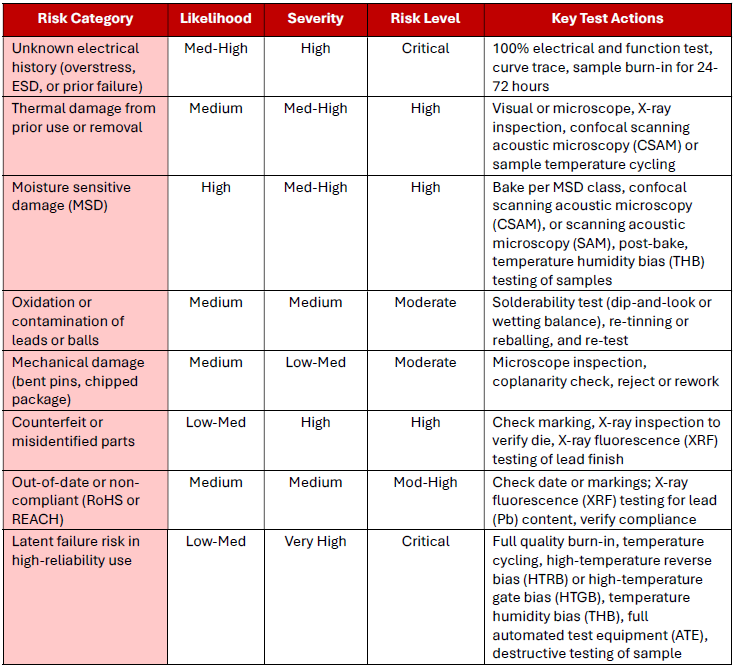
Table 2) Risk based test matrix for salvaged electronic components.
Summary
Electronic waste is a worldwide problem driven in large part by the desire of the consumer to
acquire the newest technology. As new electronic products and technology continue to rapidly
evolve, it is more critical to implement environmental and eco-friendly practices by advancing
component salvaging procedures.
The importance of using high-quality workmanship standards throughout the component
reclamation process is essential. This serves to ensure the integrity of the component supply
chain, facilitating environmental responsible practices, and reducing reliance on energy intensive
fabrication of new semiconductor devices and electronic components.
In conjunction with our ongoing electronic component reclamation activities, BEST is actively
involved with the development of the IPC-7712 Component Reclaim Standard to advance
circularity within the electronics manufacturing industry and expand the ability of component
reuse as opposed to disposal and/or recycling of electronic waste.
References
McGee, Kenny and Young, Greg, “Recycling vs Circularity: Minimizing E-Waste in Manufacturing,”
Component Sense, March 2025
Smolander, Maria and Hakola Liisa, “5 Ways to Improve the Sustainability of Electronics,” Electronic Design,
December 2023
Scanlon, Kelly and Schaffer, Mark, “Circularity Challenges in Electronics Manufacturing,” IPC and
iNEMI, July 2024
Price, Andy, LePage, Bob, Ferry, Brad, Cormier, David, “The Economics of Electronic Component
Salvage and Resue,” IPC/APEX Conference Proceedings, March 2025
Bell, Nash, “Knocking Down the Bone Pile: Best Practices for Electronic Component Salvaging,”
I-Connect007, August 2025