Mask Removal / New Pad or Trace Definition
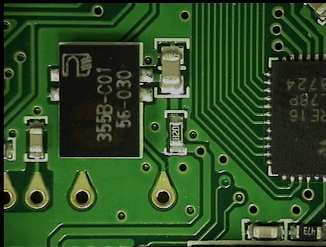
 PCB Prior to Selective Solder Mask Removal In some cases, a rework has to be performed when solder mask needs to be selectively removed from different portions of the PCB. Laser mask ablation methods have the advantage of control, cleanliness and precision over other traditional techniques such as mask scraping and micro abrasion. The BEST laser machining systems have precision and control as the beam can be lined up using the fiducials on the printed circuit board as a reference point. The fast, controllable pulse energy of the BEST laser machining systems means that the ablated mask areas will be precise and be done repeatably. The high burst of energy from the BEST UV lasers means the material is removed without charring and the mask is ablated or vaporized without remnant materials remaining on the board. In addition, because of the high energy of the laser it can very rapidly perform the solder Mask removal process.
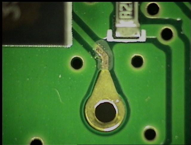
 Close Up of Extended 5mil Wide Trace In some cases, the removal of solder mask can lead to the exposure of underlying copper layers in order to “manufacture” a pad or trace. This allows for the board to be used without having to scrap or “re-spin” the printed circuit boards. Pads as small as a few mils or thousandths on a side or a trace width of 3 mils can be fabricated using the laser machining of solder mask to create a pad or trace. In some cases BEST can get the selective metal surface finish or even HASL coating placed back on the board in select area.
In other cases, pads may have to their shape or dimensions modified in order to modify the design or have a lot of boards modified in order for their design to meet manufacturability and yield standards. Micro machining using lasers to expose larger or different pad patterns will yield the desired noise or RF characteristics. In even other cases the PCB fabricator simply missed a pad or trace and one needs to be from existing with no time for a board spin. In all of these cases solder mask laser machining otherwise known as “laser solder mask ablation” can offer the precision and repeat-ability required.
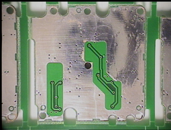
 PCB Mask Removal Other applications include cleaning up of solder mask plugged holes, silk screen removal and feature definition on the surface of the PCB. BEST lasers can also selectively cut traces or other conductors, provide the testing and subsequent coating for protection.
BEST can take data in the form of GERBERs, AutoCAD and others in order to develop both the fixturing and laser ablation files. Typically, the jobs involve several phases including process and tooling development, first article acceptance and then finally a production or lot run. BEST can provide packaging, testing, coating and part replacement services as part of the laser ablation process. During the process development of a laser rework process there may be involvement of an outside analytical lab in order to verify process parameters.
BEST knows how to handle printed circuit boards making sure that all of the IPC J-STD-001 process guidelines are followed. This mean that MSD and ESD procedures are followed as either your populated or unpopulated printed circuit boards can be reworked using laser tools.
For options on solder mask ablation methods including the use of a laser for precision solder mask removal, please call BEST today to discuss your laser mask removal or pad production application.


