Process Troubleshooting
BEST Inc provides micro-sectioning services along with professional advice to help you get to the root of process problems (Sample report). While some types of PCB assembly defects are visible, many times their extent can only be realized when micro-sectioning of the suspect area is done. Armed with this information, suppliers can be brought into the problem-solving equation and manufacturing engineering can get to the root of the problem area more quickly.

Copper dissolution at the knee where a pad meets the hole barrel
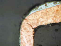
Micro-sectioning is a procedure used to prepare metallographic specimens in printed wiring boards for troubleshooting purposes. The finished prepared samples can be used for evaluating a variety of items such as the quality of the laminate system, the quality of plated through-holes, solder joint interface structures, etc. The manual metallagraphic sample preparation technique is regarded by many in the industry as an "art". It is described in IPC TM650-2.1.1 and is followed by BEST technicians.
Whether it is used alone or in conjunction with XRAY inspection methods, micro-sectioning of the PCB assembly can also provide critical information needed to make a smoother transition to lead free solder alloys. Due to this changeover the need to provide cross sections has grown for solder joints, laminates, substrates and devices to point out the issues in the changeover from tin lead. Tin based lead free alloys show vast differences in their bulk micro-structure compared to the high tin count of lead-free solders. The majority of tin-based lead free alloys exhibit inter-metallic structures within the tin-matrix which can be noted under magnification of the micro-sections.
More background information on micro-sectioning here, or or white paper here.


