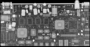
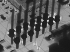
X-RAY Inspection For PCB
XRAY imaging is a widely utilized analytical tool for the SMT PCB manufacturing process. BEST will inspect your area array packages such as CGAs, BGAs, CSPs and LGAs via transmissive X-ray inspection to ensure the rework it performs meets the highest quality levels. BEST can also perform x-ray inspection of initial PCB assemblies in order to verify the process. In some cases, we can act as an inspection referee by performing x-ray inspection services on the PCB and noting any anomalies. This is a critical step in the quality control of the BGA rework process as high resolution, high magnification and high contrast X-ray images will confirm that the boards have been reworked per the industry's acceptance criteria.

Check out x-ray videos
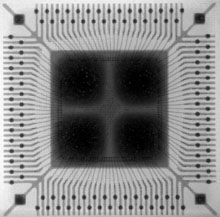
XRAY imaging, given that well-trained technicians are operating the equipment and interpreting the results, can detect a multitude of processing problems including:
- SHORTS are found using X-Ray inspection. Trained operators will make sure to note that on some double sided boards a component from the secondary side may give the appearance of a solder bridge. By rotating the board along the X and Y axis the true image can be seen and properly inspected. X-ray inspection is a common inspection method for determining shorts (non-common conductors are connected via solder).
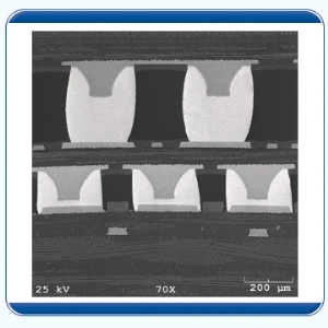
- POTATO CHIPPING occurs when a component's outside edge lifts up from a pad. This will cause the center joints to appear “flattened” and non-uniform as a result of overheating the component. This defect can be found by rotating the board on its X and Y axis allowing the x-ray technician to see the hourglass appearance of the outside edge and corner solder joints. X-ray inspection of the PCB in the device areas will determine if potato chipping is occurring.
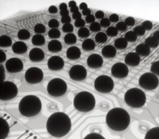
- VOIDS are the result of improper reflow profiles which exhibit entrapped flux gasses. The best way to view voids is to use a lower voltage and amperage, while the board lays flat along the X and Y axis. The technician will either manually or with the aid of analyzing software determine the percentage of void and match that against the IPC inspection criteria. X-ray inspection of leadless devices is required in order to determining the void percentage and location under leadless devices.
- POPCORNING is the breaking open or de-lidding of the package top from within the package due to moisture. The eruption may break the die from the substrate, it may pull wire bonds from pads or delaminate the package substrate itself. The x-ray technician can spot this defect when extreme cases of popcorning occur. X-ray inspection of the PCB will assist in determining whether pop-corning has occurred.
Some of the more common ones are illustrated further below:


