


Pad Repair and Circuit Trace Repair
Gold Fingers | BGA Pads | Broken Corners | Plated holes | Edges | Mask | Populated Boards | Pad and Traces
Rework/Repair Services
SURFACE MOUNT PAD AND CIRCUIT TRACE REPAIR
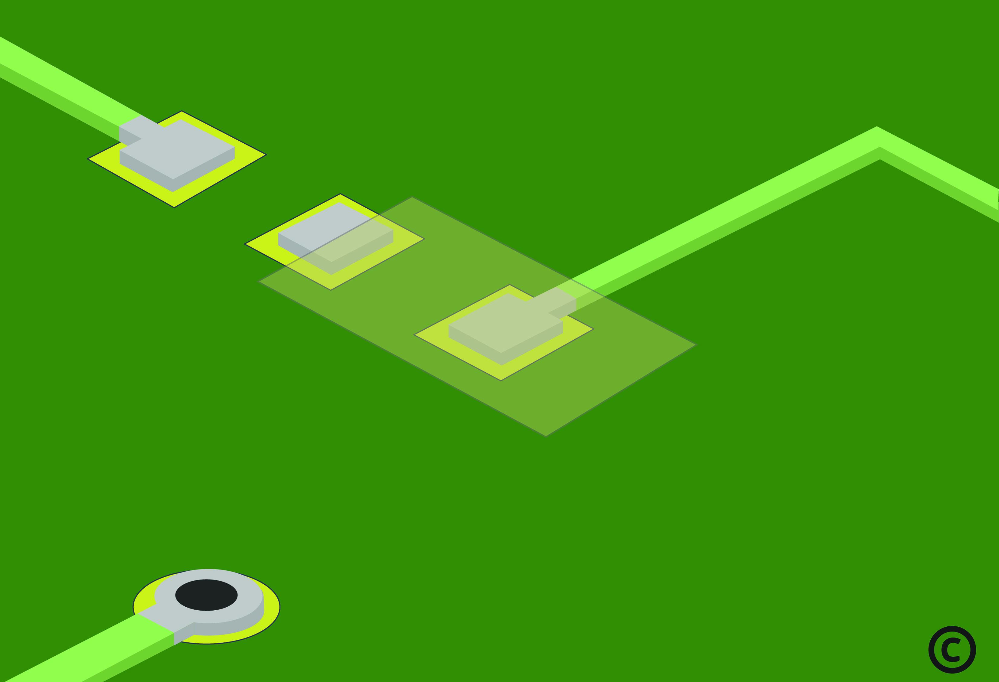
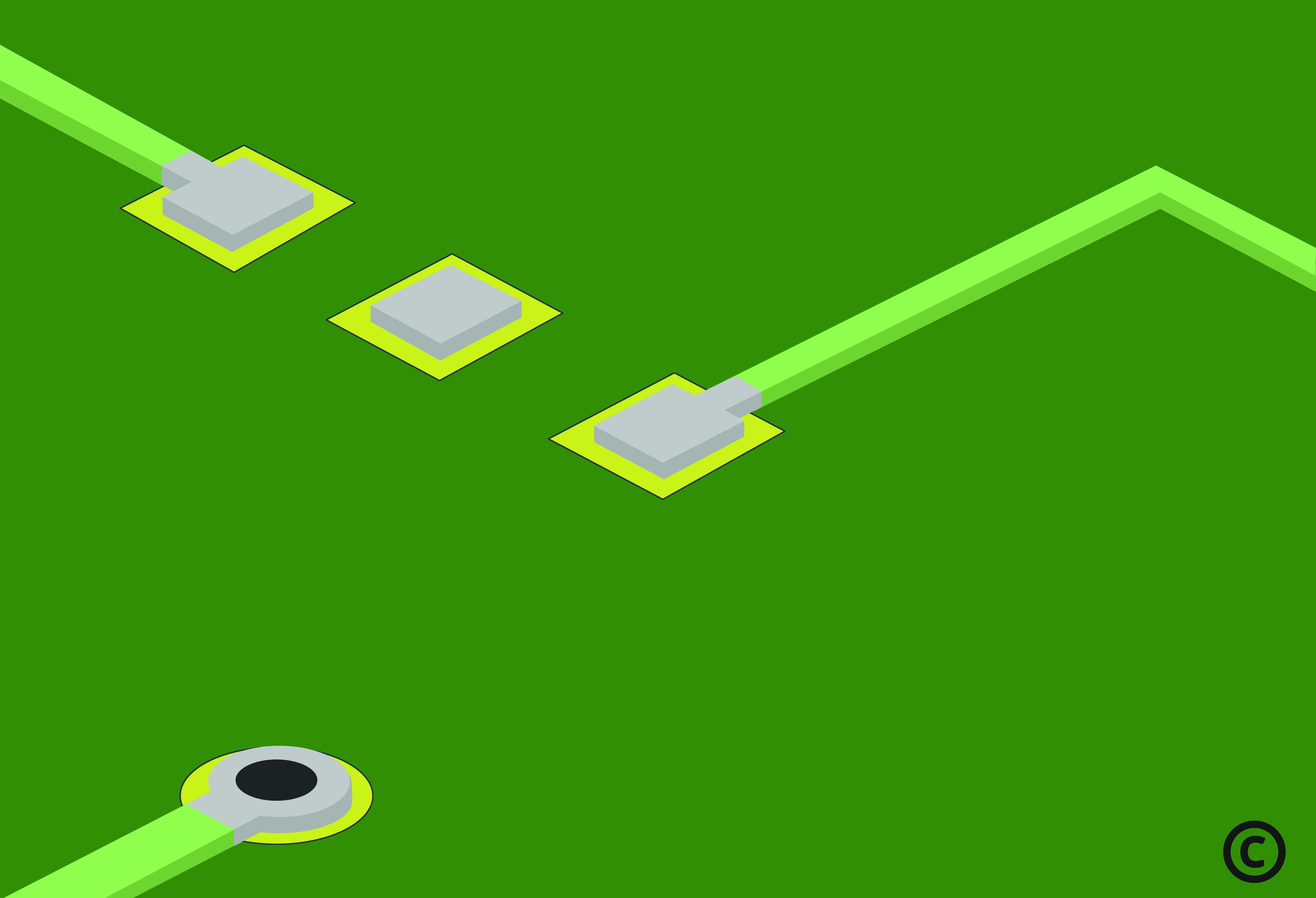
If surface mount pads, BGA pads or circuit traces have been damaged due to improper part removal techniques or mechanical "digging" into the circuit board, then BEST can repair these damaged circuit patterns to as "good as new" condition. If a critical area array device needs to have its pads and or traces repaired prior to reballing, then BEST can repair these pads and traces. If a test point was forgotten then BEST can construct a trace and pad, connecting it where you want.
BEST stocks many different kinds and styles of pads and traces in order to facilitate a fast turnaround of the repair. We even have the ability to make custom traces and pads in order to reduce the time and cost it takes to repair those boards which have the need for the same repair many times over.
BEST technicians use a variety of different IPC repair techniques along with the "tricks of the trade" they have learned over many years. This enables them to accomplish high quality repairs where only a trained eye could discern that a repair had been performed. These repair technicians are part technician and part artisan.
BEST testing has shown by using both backside micro etched circuit frames (a BEST standard) and the BEST 2-part electronics adhesive system that the bond strength of repair traces, pads and lands can approach that of the original lands, pads and traces. Even under thermal air-air shock conditions from -50°C to 85°C at a 30 minute dwell time over 200 cycles, this adhesive system performed well.
In a study summarizing a variety of adhesion techniques for the repair of printed circuit board traces, the 2 part resin-hardner epoxy system has been shown to yield the best results. Furthermore, another study demonstrated that the epoxy method yielded a greater part-pad shear strength.
If you would like to learn how to perform pad and trace repair on your own, please contact our training department and our instructors can teach you how to do this. We also have some excellent “how to” videos on our YouTube channel
 |
|
 |
 |
PCB PAD AND TRACE REPAIR GENERAL PROCESS
1.The board area requiring repair is first cleaned in and around the pad/trace to be repaired.

2.Mix with the 2-part BEST epoxy. This is a volumetric mix.
3.Carefully apply a small amount of epoxy under the entire length of the lifted circuit. The tip of an orange wood stick may be used to apply the epoxy.

4.Press the lifted pad/trace down into the epoxy and into contact with the board.
5.Apply additional epoxy to the surface of the lifted circuit and to all sides as needed for additional strength. Tape the repaired pad/trace into position while curing.
6.Cure the BEST epoxy per the instructions.
7.Re-apply conformal coating to match prior coating if it required.
8.Perform a visual examination per IPC A-610 acceptability criteria or customer requirements.
9.Perform a tape test per IPC-TM-650.
10.Perform continuity and other electrical tests as applicable.


