


Optimizing BGA Rework: Addressing Challenges, Implementing Techniques, and Ensuring Quality Control
Posted by Nash Bell on Mar 10th 2026
Since the late 1990s, ball grid array (BGA) packages have emerged as a preferred package style for
electronic devices due to their numerous advantages. Compared to high-density ultra-fine pitch
quad flat packs (QFPs), BGA packages significantly reduce the required footprint on printed circuit
boards (PCBs) by approximately 50%. The integration of standard BGAs and their stacked
counterpart, package-on-package (PoP), can further increase density, facilitating greater design
flexibility for compact and efficient circuit designs in applications ranging from consumer
electronics to automotive systems and medical devices.
Despite these advantages, the complexity of BGA packages introduces challenges during rework,
requiring innovative methods and thorough inspection practices to maintain performance and
reliability.
Abstract
BGA rework involves removing and replacing BGA packages on printed circuit boards due to
defects, upgrades, and/or failures. This process is vital for ensuring the integrity and functionality
of electronic devices. Several techniques are employed, each with distinct advantages and
considerations that must be weighed based on specific applications.
Key Terms: Ball grid array, underfill rework, device warpage, adjacent damage, mirrored BGAs,
reballing, package-on-package, solder voids, dye-and-pry testing, inspection protocols
Common BGA Rework Methods
There are many methods available for removing and replacing BGA components. The exact
method will be determined by numerous factors including available equipment, board density, and
repair technician skill level. These methods include:
- Hot Air Rework: Utilizes a stream of hot air to uniformly heat the BGA and PCB, enabling
solder melting and package removal. While effective, this method requires careful
management to prevent heat damage to adjacent components. - Infrared (IR) Rework: Employs IR emitters to directly target the BGA, minimizing thermal
impact on surrounding areas. Calibration is crucial for achieving even heating. - Vapor Phase Rework: Involves placing the PCB in a vapor-filled chamber that provides
uniform heating. This method offers excellent thermal management but can be costprohibitive
for high-volume applications. - Laser Rework: Utilizes focused laser beams for precise heating, allowing selective reflow
while minimizing damage to adjacent components. This technique requires a significant
investment in specialized equipment. - Precision Milling: Primarily used for removing underfilled components, this process
employs high-precision equipment to remove the BGA one layer at a time. While this method results in
the destruction of the component; it enables subsequent placement at
the same location and reduces the risk of pad damage. - BGA Harvest/Salvage: This process involves removing BGAs from a populated PCB and
reballing them for future use. It has gained prominence over the past five years as a
response to the chip shortage. Additionally, it serves as a more sustainable alternative to
acquiring new or costly components. - BGA Reballing: Involves removing old solder balls and replacing them with new solder balls
of a different alloy, and/or restoring electrical integrity. While cost-effective, this method
requires specialized equipment and skilled technicians. - Mini Metal and Flexible Film Stencils: Used for applying solder paste or flux during
rework. Mini metal stencils closely replicate traditional manufacturing processes, whereas
flexible film stencils offer repositionability but may have higher costs. - Stay-in-Place Stencils: These semi-permanent stencils facilitate BGA placement by
providing an accurate fit and protecting against solder shorts. However, they limit the ability
to inspect the underlying components.
Equipment and Skill Requirements
Modern BGA rework requires sophisticated machinery capable of managing small pitch sizes and
achieving precise placement accuracy. This complexity places a high demand on the skills of
technicians, who must navigate advanced rework systems effectively. Inadequate operation of
such equipment can lead to defects, while the inexperience of technicians may result in
misalignment and ultimately failed rework outcomes. These challenges underscore the
importance of having both the right tools and trained personnel to ensure successful rework
processes.
To address these challenges, investing in advanced equipment is crucial. Utilizing high-end,
programmable rework systems that offer precise temperature control and alignment can
significantly enhance success rates during the rework process. Additionally, implementing
continuous training and skill development programs will provide technicians with the necessary
expertise to operate complex machinery effectively and stay current with evolving technologies. By
prioritizing both advanced equipment and ongoing education, organizations can improve the
reliability and quality of BGA rework.
Typical BGA Rework Challenges
BGA rework carries several inherent risks that can compromise the quality and functionality of
electronic assemblies. The complexity of handling BGA components, along with the precision
required for effective soldering, increases the chances of misalignment, solder defects, and
thermal damage. Issues such as PCB delamination, cracking of the BGA packaging, and damage to
adjacent components may arise from improper rework techniques or inadequate thermal
management. Additionally, the introduction of contaminants during the rework process can
jeopardize solder joint integrity. To mitigate these risks and ensure the reliability of the final
product, it is crucial that technicians adhere to rigorous processes and quality controls in BGA
rework. Below, we provide a detailed analysis of some common challenges, associated risks, and
potential solutions.
Adjacent Device Damage
When reworking a BGA, it is essential to carefully evaluate the surrounding components, including
those adjacent to or on the opposite side of the PCB, as their proximity can significantly influence
the rework process. Whether using hot air, infrared, or other heating methods, heat-sensitive
components—such as aluminum, tantalum, and ceramic capacitors, as well as crystals,
oscillators, and plastic-bodied parts—are at an increased risk of damage or unintended reflow due
to localized or excessive heat exposure. These components may have different thermal tolerances,
and improper temperature control can cause them to deteriorate, lose functionality, or become
physically damaged.
To mitigate these risks, it is important to employ precise temperature profiles, targeted heating
techniques, and strategic cooling to limit heat diffusion to sensitive areas. Additionally, using
physical barriers or heat shields can protect vulnerable components during the rework process.
Implementing careful process control, along with thorough pre-rework inspection and planning,
ensures the integrity of the entire assembly while effectively reworking the BGA.
From a process standpoint, the choice of heat source during rework is a critical factor that can
significantly impact the success of the procedure. When using an automated rework station, it is
essential to select an appropriately sized and shaped nozzle that provides targeted and uniform
heat application without encasing or inadvertently heating nearby components. An ill-fitting nozzle
can lead to uneven heating, increased thermal stress, or damage to adjacent parts. Employing low
temperature rework methods that include preheating the entire board or specific areas before
direct heating of the BGA can effectively reduce thermal gradients and minimize stress on both the
component and the PCB. Preheating helps elevate the overall temperature gradually, making the
localized reflow more controlled and reducing the risk of warpage, pad lifting, or delamination.
Additionally, incorporating precise temperature control, optimized airflow, and proper fixture
support ensures that heat is delivered efficiently and evenly. By carefully selecting the heat source,
nozzle size, and employing preheating techniques, technicians can achieve a reliable rework
process that maintains the integrity of the assembly while minimizing potential damage.
Large BGAs
As devices continue to increase in complexity and computing power, larger BGA packages—up to
125 mm x 125 mm—have become more common, posing significant challenges for rework. BGA
rework systems typically rely on split vision prism technology for alignment, but these systems are
often ill-equipped to handle oversized packages, requiring upgrades for reliable rework.
Additionally, bottom heaters need to be enhanced to ensure even and uniform heating of the
board, as undersized heat sources can create temperature gradients that lead to issues such as
elongated or stretched component balls and cold peels. These problems can damage BGA pads on
the PCB and compromise the rework process due to improper temperature control.
Another significant challenge is maintaining a consistent temperature across the entire surface
area of large packages during rework. Airflow turbulence from hot air rework nozzles can result in
fluctuating temperatures, limiting their effectiveness in achieving uniform reflow. Moreover, many
commercially available infrared (IR) rework systems lack the appropriate spot size necessary to
adequately heat such large components, further complicating the rework process.
To overcome these challenges, technicians can employ several strategies. Custom-machined
board supports specifically designed for larger packages can enhance stability during rework.
Implementing stay-in-place stencils can improve solder paste application, thereby expanding the
process window. Additionally, a thorough understanding of proper thermal profiling can assist
technicians in optimizing older machines to accommodate larger packages, albeit with some
limitations. By addressing these challenges proactively, rework technicians can enhance the
efficiency and effectiveness of BGA rework processes for larger devices.
Underfilled BGAs
Underfill is typically composed of either epoxy or polymeric-based material that is dispensed under
electrical components such as BGAs. This material is designed to protect devices from mechanical
forces and mitigate the effects from coefficient of thermal expansion (CTE) mismatches between
the device and the printed circuit board (PCB) or between the die and the substrate in flip chip
packages (see Figure 1a). While underfill is highly effective in protecting components, it presents
significant challenges when rework is required (see Figure 1b).
Rework methods that involve hot air are generally not recommended for underfilled components.
Heating the underfill to near reflow temperatures causes it to become liquidous, which can impede
the formation of reliable solder connections.
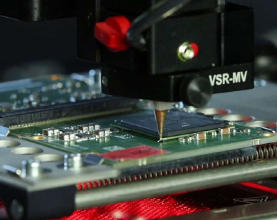
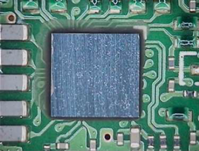
Fig. 1a) BGA underfill operation on PCB assembly (left), and 1b) underfilled ball grid array (right)
Several methods can be employed for reworking underfilled BGAs, each carrying its own set of risks
and challenges. The most common approach involves applying targeted heat to reflow the BGA,
which softens the solder joints and allows for removal or repositioning of the component. During
this process, a critical step is creating a controlled parting line in the underfill material between the
BGA and the PCB, typically achieved through precise heating and mechanical separation
techniques. This method requires careful control of temperature and application force to prevent
damage to the PCB pads or the underlying traces, as excessive heat or force can lead to
delamination, pad lifting, or damage to adjacent circuitry. Additionally, improper execution can
result in incomplete removal of the underfill or residual debris, which can interfere with re-balling
or reattachment. Because of these risks, this method demands skilled technicians, specialized
equipment, and meticulous process control to ensure successful rework without compromising
the integrity and reliability of the assembly.
Another effective technique involves the use of a specialized softening agent designed to reduce
the adhesive strength of the underfill material, thereby facilitating easier removal of the BGA (see
Figure 2a). This approach typically entails applying the softening agent precisely to the underfill
area, where it penetrates and weakens the bond between the underfill and the PCB or the BGA
itself. By decreasing the adhesive force, technicians can more safely and efficiently lift or detach
the component without exerting excessive mechanical force, which could otherwise damage the
PCB pads, traces, or neighboring components. This method minimizes the risk of collateral
damage associated with mechanical separation and helps preserve the integrity of the circuit
board. The softening agent is often chosen based on compatibility with the specific underfill
material and the temperature profile of the rework process, ensuring effective performance without
leaving residues that could interfere with subsequent rework steps, such as cleaning, re-balling, or
reattachment. Proper application and controlled process parameters are essential for maximizing
the benefits of this technique while minimizing potential risks.
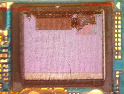
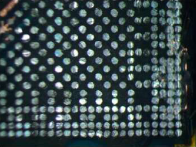
Fig. 2a) Softening agent used during underfill rework (left), and 2b) BGA pads after milling of underfill (right)
When salvaging the component is no longer an option, “cold milling” may provide a viable
alternative (see Figure 2b). This method involves cutting away the component in thin layers, leaving
only residual solder on the pads. The remnant material can be easily removed to prepare for
subsequent placement of a new BGA. This process requires specific equipment and training for
optimal results.
Component and PCB Warpage
Warpage occurs when components are exposed to significant temperature changes in a short
period of time. Factors such as the rate of temperature change, moisture exposure, and the size
and thickness of the components all contribute to the degree of warpage. When BGA warpage
occurs, the corners typically experience the greatest displacement, resulting in defects such as
opens or solder bridging.
Once a component or PCB is warped, several strategies can be employed to counteract or
minimize the effects of warpage during rework or assembly. One effective approach is the use of a
custom fixture or loading device—such as a clamping jig or a controlled pressure system—that
gently applies force to flatten the component or PCB, holding it in a flat position during reflow or
soldering. This helps redistribute stresses evenly and maintains proper contact with the PCB pads.
Additionally, applying localized heat with a focused heat source to areas of warpage can help relax
internal stresses and slightly reduce warping. Using thermal cycling—gradually heating and cooling
the assembly—may also relieve residual stresses over time. In some cases, applying a conformal
coating or supportive overlay material after reflow can help stabilize the component or board in a
flat position. Combining mechanical, thermal, and fixture-based methods is often the most
effective way to mitigate warpage issues and ensure reliable electrical and mechanical
connections.
Additionally, the J-STD-033 and JEDEC guidelines offer recommendations for handling moisturesensitive
devices, outlining prebaking and storage procedures that can significantly reduce the risk
of warpage. Following these standards helps ensure greater reliability in electronic assemblies.
Fine Pitch Micro BGA Device Warpage
High-density synchronous dynamic random-access memory (SDRAM) devices are typically housed
in a fine pitch micro ball grid array (μBGA) package. A standard package size for a 96-ball SDRAM is
7.5 mm x 13.3 mm, featuring a 0.8 mm ball pitch and a 0.48 mm ball diameter (see Figure 3a).
These devices are very thin, measuring only 1.4 mm in thickness, and are prone to warpage when
mounted on double-sided PCBs that undergo two reflow cycles, as well as elevated temperature
cycles during burn-in and/or functional tests (see Figure 3b).
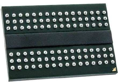
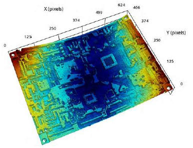
Fig. 3a) 96-ball SDRAM μBGA device (left), and 3b) shadow moiré measurement of μBGA warpage (right)
Warpage of a μBGA can reach up to 40-microns and is typically more pronounced along the major
axis of the 7.5 mm x 13.3 mm rectangular package. This warpage causes the top surface of the
device—the side without the solder balls—to become concave, while the bottom surface—the side
with the solder balls—warps in a convex direction. As a result, this induces a force in the Z-axis
direction, leading to random ball shearing between the solder balls and the μBGA interposer, which can be confirmed through boundary scan testing (see Figure 4a). Defect mapping shows that the
highest occurrence of these anomalies is typically at the end and corner balls (see Figure 4b).
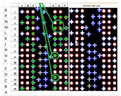
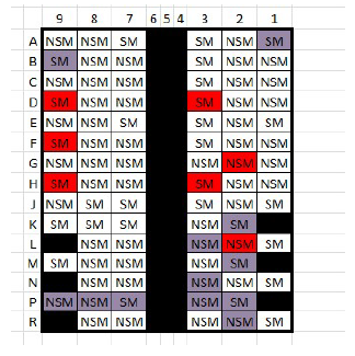
Fig. 4a) Boundary scan test summary (left), and 4b) mapping of random boundary scan defects (right)
Component warpage can be exacerbated by using a 4-mil (100-micron) stencil and a solder paste
inspection system with an upper limit set at 165% and a lower limit at 50%. In some cases, this may
result in a solder deposit that is only half of what is required, leading to an interconnection with
insufficient mass and strength. A 50% deposit of a 100-micron solder paste can pass inspection even
at a thickness as low as 50-microns, which is inadequate for a μBGA device with a potential warpage
of 40-microns. Consequently, this can cause random opens, microfractures (see Figure 5a), and
separation of corner balls (see Figure 5b).
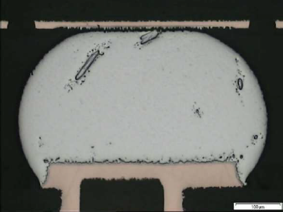
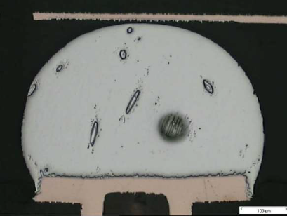
Fig. 5a) Micro fracture between μBGA ball and μBGA (left), and 5b) separation of corner μBGA ball (right)
Additionally, the combined use of non-solder mask defined (NSMD) pads and solder mask defined
(SMD) pads on a single BGA component should be minimized or avoided. Inconsistent application
of NSMD and SMD pads can lead to variations in molten solder height, which may contribute to
uneven joint strength. Solder mask defined (SMD) pads are recommended only for BGAs with
pitches below 0.4 mm (0.016”) and for bottom-terminated leadless (BTL) components, such as
land grid arrays (LGA) and quad flat pack no-lead (QFN) devices.
Mirrored BGAs
When BGAs (see Figure 6a) are placed back-to-back on opposite sides of a two-sided PCB, this
configuration is known as BGA mirroring. It presents challenges due to the increased density in the
rework area. Typical rework methods involve preheating the board to at least 125°C using a heat
source located beneath it. In the case of mirrored BGAs (see Figure 6b), this process can expose
the underside component to prolonged heat, increasing the risk of damage and warping.
Additionally, it may cause the underside component to enter reflow, resulting in solder anomalies,
joint embrittlement, and potentially leading to heavier components detaching from the board.
Fig. 6a) BGA device before mounting (left), and 6b) mirrored or back-to-back BGAs on PCB assembly (right)
To overcome the challenges posed by mirrored BGAs during rework, careful planning and targeted
techniques are essential. One effective strategy is to utilize localized heating methods, such as
infrared (IR) or hot air rework systems with precise temperature control, to minimize heat exposure
to surrounding components. Employing thermal shields, such as aluminum foil or specialized
thermal pads, can protect the underside BGA from excessive heat during the rework process.
Additionally, using low-temperature solder materials or techniques that allow for shorter heating
cycles can significantly reduce the risk of damage and warping. Implementing careful monitoring of
temperature profiles throughout the rework can help ensure that each component is subjected to
optimal conditions for solder reflow without compromising the integrity of adjacent parts. Such
measures can effectively mitigate the risks associated with reworking mirrored BGAs on two-sided
PCBs.
Package-on-Package
Package-on-package (PoP) is an advanced electronic-stacked package architecture that involves
vertically stacking ball grid arrays (BGAs), most commonly in a two-high configuration. In this
setup, the package closest to the circuit board is typically the logic or CPU module, referred to as
the bottom package (see Figure 7a). The top package sits directly above, serving as the memory
module. This stacking arrangement allows for a compact, high-density design, making it especially
suitable for portable and space-constrained devices. PoP configurations are prevalent in consumer
electronics such as smartphones, tablets, and netbooks due to their ability to integrate high I/O count, fine pitch, and very thin packages within a small footprint. These packages are designed to
support high-speed data transfer and electrical performance while maintaining a slim profile,
which adds to their popularity in modern, space-efficient electronic devices.
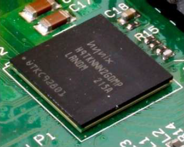
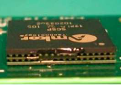
Fig. 7a) Package-on package device (left), and 7b) physical damage to PoP device before rework (right)
Reworking PoP (package-on-package) BGAs presents several unique challenges due to their
stacked configuration and fine-pitch design. First, the proximity of the top and bottom packages
means that applying heat during rework must be carefully controlled to avoid damaging either
package or the underlying PCB. Excessive or uneven heating can cause warpage, delamination, or
solder joint failure, especially given the very thin and high I/O density of these packages.
Second, the stacked architecture complicates access. Removing or replacing the top memory
package requires precise alignment and controlled reflow to prevent disturbing or damaging the
bottom logic or CPU package. The close spacing makes mechanical handling difficult and
increases the risk of physical damage during the process (see Figure 7b).
Third, warpage and internal stress are common issues, especially in temperature cycling or
multiple reflow attempts. Warping can cause misalignment, resulting in poor solder joints or open
connections, which are difficult to detect and repair.
Fourth, the presence of fine pitches and small ball sizes adds to the difficulty, raising risks of
bridging, micro-cracks, or incomplete solder wetting during reflow. The tight spacing also leaves
limited room for applying rework tools or fixtures and complicates inspection.
Overcoming the rework challenges associated with PoP BGAs requires a combination of precise
process control, specialized equipment, and skilled technicians. Initial steps include thorough prerework
inspection using advanced imaging techniques such as X-ray or 3D inspection to assess
warpage, solder joint integrity, and component alignment. Controlled and localized heating with
rework stations, designed for fine-pitch and stacked packages, helps prevent overheating and
warpage. Employing pre-heating and gradual temperature ramping reduces thermal and internal
stress that could lead to delamination or damage. The use of custom fixtures, vacuum supports, or
mechanical clamps stabilizes the PCB and PoP modules during reflow, maintaining proper alignment
and minimizing warpage or physical distortion. Gentle, controlled mechanical removal
techniques are essential to avoid damaging delicate solder joints or substrates. Process
parameters such as solder paste application and reflow profiles must be carefully optimized for
the small ball sizes and pitches typical of PoP packages. Real-time temperature monitoring and
feedback controls further ensure uniform heating, reducing the risk of uneven thermal expansion
and component cracking. Skilled personnel trained in handling stacked, fine-pitch packages, along
with rigorous post-rework inspection using boundary scan, X-ray, or 3D AOI, ensure the integrity of
joints and alignment before final assembly or powering up. By implementing these strategies,
manufacturers can effectively address the complexities of PoP BGA rework, improving yields and
ensuring reliable operation of the finished assembly.
BGA Reballing
Reballing BGAs is an integral step in BGA rework. This process involves removing the original
solder balls from a BGA and replacing them with new ones. This step is utilized when the goal is to
reuse the original BGA either on the same board or for component salvage. BGA reballing can also
be utilized with unused components that require a different solder alloy or with solderability issues
such as solder ball oxidation.
The first step in the reballing process involves removing the original solder balls to expose the pads.
BGA deballing can be accomplished manually or robotically. Manual deballing is performed by
wicking the solder balls using a soldering iron and copper braid. While this is an effective and
commonly used method, there is potential risk of damaging pads if not performed properly.
Robotic deballing is performed using a robotic hot solder dip (RHSD) machine equipped with a
dynamic solder wave (see Figure 8a). A single wave stripping process is adequate providing the
solder wave has sufficient scrubbing action to completely remove the original solder balls (see
Figure 8b). Since robotic deballing is touch-free, the risk of scratching pads is significantly
reduced, however due to the extreme temperature of the molten solder wave, this process may
result in defects such as lifted pads.
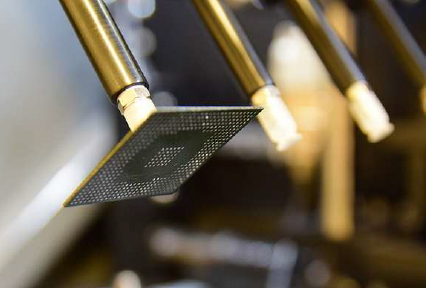
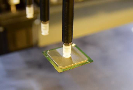
Fig. 8a) Ball grid device before automatic de-balling (left), and 8b) ball grid array being de-balled (right)
Once the BGAs have been successfully deballed, the next step is to attach new spheres to the
component, for which several methods are available. A common ball placement method involves applying
tacky flux to the component and using a fixture that matches the component’s array (see
Figure 9a). The fixture ensures proper ball alignment, while the flux helps secure the balls in place
for reflow.
Another option is to use reballing stencils or preforms, made of high-temperature plastic and preloaded
with balls that match the component's pattern. This single use preform is easily aligned on
the component and placed in the reflow oven for ball attachment. Reballing BGAs using stencils
does not require expensive equipment and can be trained with relative ease.
Automated laser-based BGA component reballing systems offer a relatively new ball attachment
option. This process uses a cone-shaped nozzle that holds a single solder ball. When the nozzle tip
is aligned at the desired location, a laser targets the solder ball, making it malleable enough to fall
through the nozzle and adhere to the BGA pad. This method is designed to be both efficient and
highly precise, capable of handling pitches as fine as 0.4 mm (see Figure 9b). However, the
equipment requires a substantial investment and is better suited for attaching balls on virgin parts
rather than those that have been deballed, as even minor pad oxidation can lead to defects.
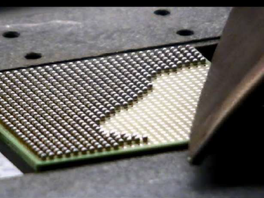
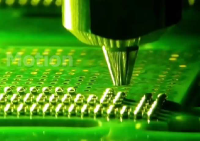
Fig. 9a) BGA reballing via custom fixture (left), and 9b) fixture-less 0.4mm pitch laser BGA reballing (right)
Following the deballing and reballing processes, inspection should be carried out including
verifying device coplanarity, missing solder balls, solder ball volume, shorts between adjacent
solder balls, and detection of any foreign object debris. A reliable reballing process is a vital step to
ensuring high quality rework of BGAs.
Inspection for BGA Rework
Effective inspection of BGA solder joints post-rework is essential to ensure the reliability of
connections and overall performance of electronic devices. Different methodologies offer various
insights into solder joint quality and potential issues, each suited for specific applications.
Visual Inspection
Visual inspection is a critical first step in assessing solder joint quality, and it is vital to conduct
these inspections according to the IPC-A-610 standard to ensure compliance and reliability.
Technicians often utilize magnification tools, such as microscopes or borescopes, to closely
evaluate solder terminations, alignment, and any visible defects. Key considerations for effective
inspections include selecting the appropriate level of magnification, ensuring adequate lighting,
and maintaining a controlled environment. Common defects that inspectors should look for
include missing solder balls, ball size, solder bridging, and improper wetting, as these issues can
significantly impact the performance and durability of the solder joints. Implementing thorough
visual inspections is essential for achieving high-quality rework outcomes.
X-ray Imaging
X-ray inspection is a valuable non-destructive method for evaluating the internal structure of solder
connections, particularly for hidden joints beneath BGAs. This technique is crucial for identifying
issues that may not be visible during visual inspection such as shorts, opens, and head-in-pillow
defects (see Figure 10a). To enhance the effectiveness of X-ray inspections, it is essential to follow
proper procedures, including capturing images from multiple angles and using appropriate
magnification for detailed views of the solder joints (see Figure 10b).

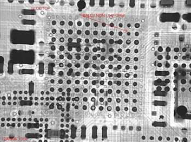
Fig. 10a) Defects visible via X-ray Inspection (left), and 10b) X-ray image of undersized solder balls (right)
Additionally, it is essential to ensure that the X-ray inspection system is properly calibrated
regularly to maintain accurate imaging and defect detection capabilities. Calibration involves
adjusting the system to account for any drift or discrepancies in imaging resolution and contrast,
which is critical for reliably identifying subtle defects. Equally important is providing
comprehensive training for technicians in image analysis techniques. Skilled operators who
understand how to interpret X-ray images can distinguish between acceptable variances and
actual defects such as solder bridges, voids, or insufficient solder joints (see Figure 11a and 11b).
Proper training enhances the ability to detect hidden internal issues that could compromise
product reliability, thereby reducing the risk of undetected failures in the final assembly. Together,
precise calibration of the equipment and well-trained personnel dramatically improve the
effectiveness of X-ray inspection, leading to higher quality assurance and more reliable electronic
assemblies.

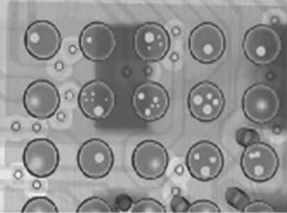
Fig. 11a) Oversized solder balls detected by X-ray (left), and 11b) solder voids in enlarged field-of-view (right)
Dye and Pry Testing
Dye and pry testing is a highly valuable, yet inherently destructive method used to evaluate the
quality of solder joints, particularly in BGA rework applications. This technique involves applying a
penetrating dye to the solder joints, which will seep into cracks, voids, or areas of insufficient
coverage, providing visual evidence of potential defects. Subsequently, a controlled mechanical
force is used to pry the BGA package away from the PCB, allowing technicians to observe the site
and assess the integrity of the solder connection. As the package is lifted, the dye reveals gaps,
cracks, or voids along the joint interface, offering critical insights into the reliability of the solder
bond (see Figure 12a).
Due to its invasive nature, dye and pry testing is typically reserved for diagnostic purposes, failure
analysis, or critical quality inspections, as it permanently damages the component and PCB. To
ensure accurate and repeatable results, it is important to follow proper procedures, including an
even dye application and controlled force during the pry operation. Trained technicians must also
be proficient in interpreting the visual evidence, which helps identify potential weaknesses in
solder connections. Overall, dye and pry testing enables organizations to detect hidden defects
that could compromise long-term performance, thereby supporting improved quality control and
ensuring the dependability of electronic components (see Figure 12b).
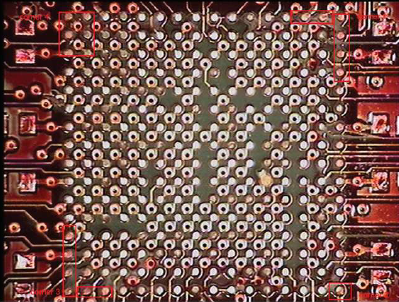
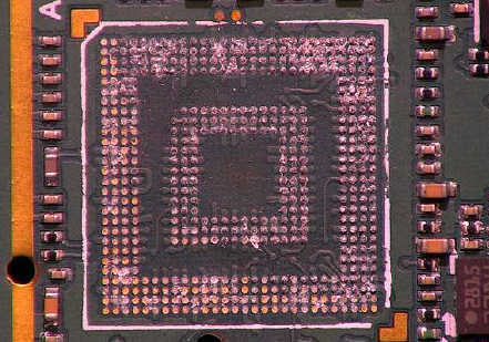
Fig. 12a) Dye penetration in corners of BGA (left), and 12b) open connections due to BGA warpage (right)
Summary
BGA rework is often regarded as a necessary, yet inherently challenging aspect of electronic
manufacturing. Since it is rarely planned during the initial design phase, rework procedures
frequently involve overcoming a variety of obstacles that were not anticipated. Successfully
navigating these challenges depends heavily on operator experience, the use of advanced
equipment, and sometimes thinking creatively to develop effective problem-solving
strategies. The process is further complicated by factors such as underfilled components,
warpage, and the proximity of neighboring devices, all of which require careful consideration
and strategic approaches during rework. Due to the inherent risks—such as warpage,
misalignment, or damage to delicate components—employing a combination of carefully
designed mitigation techniques is essential to achieving a successful outcome. This complex
task is typically refined over many years of trial and error, learning from failures to develop
best practices.
To uphold high standards of quality, it is also crucial to invest in advanced equipment,
provide ongoing technician training, and implement rigorous inspection protocols. As BGA
technology continues to evolve, addressing these challenges through innovation and skill
development will be vital for ensuring reliable repair operations and maintaining the
performance of electronic devices in a rapidly changing industry landscape.
References
Gaynor, Adam and Wettermann, Bob, “Shielding Effectiveness of Polyimide Tape During Rework,”
Circuits Assembly Magazine, October 2014
Wettermann, Bob, “Knocking Down the Bone Pile: Top Challenges in BGA Rework,” I-Connect007, March
2023
Henry, Reid, “The Critical Role of Robotic Hot Solder Dip Processing of Components for High-
Reliability and Missions-Critical Applications,” Hentec Industries/RPS Automaton, July 2023
Wettermann, Bob, “Knocking Down the Bone Pile: BGA and PCB Warpage – What to Do,” I-Connect007,
July 2019
Zarrow, Phil and Klenke, Bob, “Mitigation of Solder Ball Shearing Defect Investigation Summary Report,”
ITM Consulting, December 2012
BEST Inc.
3603 Edison Place
Rolling Meadows, IL 60008
Email: nash.bell@solder.net
Phone: (847) 797-9250