PCB X-ray Inspection in Real Time
Older trans-missive top-down (2D) X-ray systems are inadequate to inspect and detect many common modern PCBA defects. Even painstaking fixturing samples on edge do not always yield the view you want. In addition, the smaller-sized devices and dimensions on PCBAs today require very small spot sizes and high magnification-something the older style systems cannot “see”. The inspection criteria and complexity of devices require more sophisticated inspection software capable of many calculations. The complexity and size, as well as RF shields with components underneath, stacked packages, multi-row connectors and other devices, make PCB x-ray inspection ever more challenging.
BEST newest PCB x-ray capabilities answer these modern challenges. Offering real-time, off-axis x-ray, our system is designed specifically for x-ray inspection of PCBs, whether for failure analysis or for production inspection. Samples can be manipulated with a 360 degree rotational axis, and up to 75 degree oblique viewing angle, while the powerful software allows operators and engineers to visualize the most challenging assemblies. These capabilities allow for you to see all of your PCB assembly during the x-ray inspection process.
PCB x-ray inspection today is a necessity on modern printed circuit boards as there are many devices which have non inspectable surfaces. Chief amongst the solder joints with non visually inspect-able surfaces include both ball grid arrays as well as bottom-terminated components. X-ray PCB inspection allows you to both make calls in terms of the inspection criteria as well as measurements. PCB x-ray inspection also allows you to “see” solder voids (including measurements) as well as solder anomalies like non-wetting solder balls. Other uses of these x-ray images include determining the hole fill of plated through-hole solder joints without destructive testing like cross sectioning. Another useful phenomenon which can be seen is the wetting characteristics of solder on pads underneath a component or that remain hidden to the eye because of the density of the printed circuit board. All of these criteria and more can be noted with a proper view of the printed circuit board during x-ray inspection.
Below are some sample images and applications:
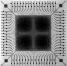
X-Ray Image of a QFN with dual IO Rows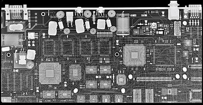
Entire PCBA is “Mapped” prior to individual locations being inspected for AXI
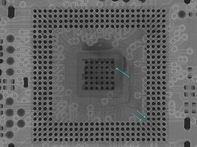
Irregular Solder Balls
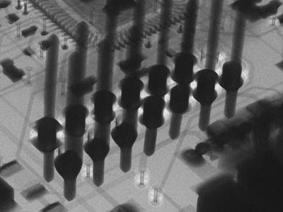
Plated Through-hole Inspection