Overview Benefits Instructions Void Reduction

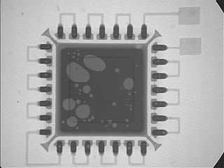
X-Ray image indicating large center void grounds present
There are several problems in reworking lead-less devices. The device, without the proper “channels” for the out-gassing flux volatile to escape, can build up a lot of solder voids during the reflow process. These voids could lead to opens at the interconnection point between the device and the PCB. In addition, the larger area of the ground plane tends to crown and “lift up” the device in the center vis-a-vis the outlying IO thereby creating opens are no-connects on the periphery of the device.
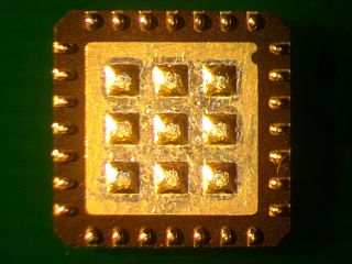
By “bumping” the device using a properly window-pane center ground area the right “channels” for these volatiles are created for escape. This in turn leads to less voiding. In addition these “bumped” areas as all of similar height and therefore upon reflow the devices do not “tilt” and cause IO opens to form.
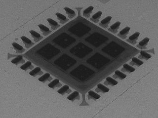
This is a x-ray image is of a “bumped” QFN showing that the ground pad is very few solder voids and that the connects to the IO points are continuous.
This is a picture of the device after it has been “bumped” and placed using the StencilMate™ method. Not only is the process simplified and the process window widened but the voids are reduced and the interconnection problems are lessened.


