BEST PCB REPAIR CIRCUIT FRAMES
WHY BEST PCB REPAIR CIRCUIT FRAMES?
- Stock to 5 business day delivery - every part of the process is controlled in house. ORDER HERE.
- Consistent quality of the circuit frames as all processing is done in house
- Wide variety of materials - gold plated as well as both 1oz and 2oz copper frames with tin coating for RoHS compliance
- Custom frames available as processing is done in house-saves your technician’s repair time, reduce the minimum order quantities and significant tooling charges and specialty tooling The base metal can be either is 1 or 2oz copper with chemical etchant which allows for high bond strength to the PCB which will be repaired. The dimensions of the standard frames are 60 x 40 mm. The coating on the PCB side is either a shiny tin of nickel or gold coating. The film is a low stress epoxy film adhesive with a Tg at –60ºC. This minimizes the thermal stress on bonded parts during thermal cycling or shock testing from –55 to 150ºC. It is a clear materials, nearly 1mil (0.0254mm) in thickness. It has a shelf life of 6 months minimum and is date-coded on the circuit frame to which it is bonded.
- Epoxy and Dry Film Circuit Frame - you have a choice! Dry Film Adhesive System - A clean way that damaged pads and traces can be replaced without the mess of liquid epoxy. The BEST replacement circuit frames with dry-film adhesive backing make this repair process clean and neat. Simply trim out the circuit you need and bond it to the circuit board surface using heat and pressure. The BEST dry film is superior to others as it is very clear. This makes it easy for the repair technician to see what is going on to align the pad or trace to the PCB. In addition, the BEST dry film is thinner than others, making it sit on the PCB post repair closer in height to the original pads or traces. This makes for a neater repair! If you are already using a dry film epoxy system, see our competitive cross-reference chart here.
- Epoxy Adhesive System - Proven reliability BEST testing has shown by using both backside micro-etched circuit frames (a BEST standard) and the BEST 2-part electronics adhesive system that the bond strength of repair traces, pads, and lands can approach that of the original lands, pads, and traces. Even under thermal air-shock conditions from -50C to 85C at a 30 minute dwell time over 200 cycles, this adhesive system performed well. In a study summarizing a variety of adhesion techniques for the repair of PCB traces, the 2-part resin-hardner epoxy system has been shown to yield the best results. See the results here.
| Frame Size: |
57 x 38 mm (2.25" x 1.50") |
| Material: |
Copper foil 0.036 mm (0.0014")-backside micro-etched for enhanced adhesion |
| Adhesive Backing: |
Phenolic film adhesive 0.0254 mm (0.001") thick. |
| Electrical Resistivity: |
Greater than 1014 ohm-cm |
| Dieletric Strength : |
750 Volts/mil |
| Glass Transition Temperature: |
-60º C |
| Device push off strength: |
Greater than 2,000psi, or 13.8N/mm2 |
| Peel Strength: |
Greater than 9lbs/in (1.61 kg/cm) post cure to FR-4 |
| Hardness: |
65 Type A |
| Cured density: |
1.2 gm/cc |
| Thermal Conductivity: |
1.2 BUT-in/hr-ft2-ºF |
| Linear Thermal Expansion: |
110 ppm/ºC |
| Max Continuous Oper Temp: |
150ºC |
| Bonding Time: |
15 seconds |
| Bonding Temperature: |
200ºC |
| RoHS compliance: |
YES |
| Shelf Life: |
6 months min. Circuit Frames are laser engraved with the expiration date. |
WHY BEST PCB REPAIR MATERIALS?
Flexibility to Meet Your Requirements
- Lead-Free/RoHS compatible
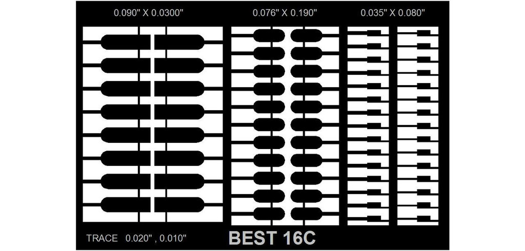
- BEST can help you become more proficient at PCB repairs by offering a wide variety of tools to reduce the amount of time spent trimming circuit frames. Choose from a large variety of our different pads, traces, contact fingers and land patterns... or let us make a specialized version for you! We can turn these specialized patterns around for you quickly-as they are manufactured in house!
The right tools for the right job
- BEST can help you become more proficient at PCB repairs by offering a wide variety of tools to reduce the amount of time spent trimming circuit frames. Choose from a large variety of our different pads, traces, contact fingers and land patterns... or let us make a specialized version for you! We can turn these specialized patterns around for you quickly-as they are manufactured in house!
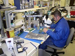
Because BEST PCB repair kits are designed by artisans who repair circuit boards for a living the right tools have been included in our PCB repair kit. BEST Inc. PCB repair artisans have been involved in board level repairs for a combined 60 plus years. In addition, several BEST Inc staff members have been teaching and contributing to the procedures found in the IPC "7721 Repair and Modification of Printed Boards and Assemblies". This combined real life experience is captured through a series of "how to" slides which will guide you through the actual repair procedures. These instructions provide advanced repair technicians some "tricks of the trade" which are key when performing PCB repairs.