 |
|
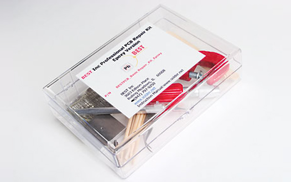
The BEST PCB Repair Kit is designed to meet the quality of original trace, pad and plated thru-hole assemblies.
BEST PCB repair kits give you the tools you need for fast repair and modification of lands, traces, contact fingers, SMT pads, plated hole connections and PCB base board material. These materials, packaged together and designed by one of the premier PCB repair companies, BEST Inc., allow you to meet original PCB quality standards.
This is the most complete kit for your printed circuit board repair needs and includes not only the material required for such repairs but also professional "how to" instructional slides. It's the total package. This kit includes a selection of eyelets and funnelets, swaging tools for eyelets, a variety of circuit frames to repair or add traces, SMT pads, through hole connections and edge connectors. This kit can be had in either a dry film or epoxy versions for the pad and circuit trace repairs.In the dry film version a soldering iron and operator pressure make the connection while in the epoxy version a 2-part epoxy is mixed and applied to replacement pads and traces. Each kit also contains a variety of specialty tools which, are used by both BEST Inc professional repair technicians and as teaching aids for board level repair instructors. If you need to repair damaged circuit boards, the all-in-one kit is just what you need.
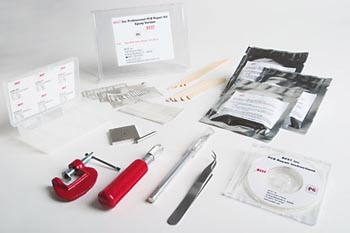
| Quantity Included in Kit | Description |
| 3 | Resin/Hardner, 2gms with divider |
| 5 | Popsicle sticks for clamping down for PCB repairs, 10 count |
| 5 | Orange sticks for mixing, 10 count |
| 1 | Swaging tool for through hole repairs-base |
| 1 | Swaging tool for through hole repairs-fixture |
| 2 | Dental pick for scraping off burnt tracks/laminate |
| 1 set | Large knife with assorted blades |
| 1 set | Small knife with assorted blades |
| 1 | 1" c-clamp for holding epoxied tracks in place |
| 50 | Eyelet .021" ID, .030" OD, .078" LUF 50 pcs |
| 50 | Eyelet .034" ID, .046" OD, .093" LUF 50 pcs |
| 50 | Eyelet .058" ID, .068" OD, .102" LUF 50 pcs |
| 50 | Eyelet .026" ID, .040" OD, .093" LUF 50 pcs |
| 50 | Eyelet .064" ID, .076" OD, .091" LUF 50 pcs |
| 50 | Eyelet .048" ID, .059" OD, .093" LUF 50 pcs |
| 1 | SMT Pad Circuit Frame, tin plated, for epoxy use |
| 1 | Edge Connector Circuit Frame, tin plated, for epoxy use |
| 1 | Trace Circuit Frame, tin plated, for epoxy use |
| 1 | Through Hole Circuit Frame, tin plated, for epoxy use |
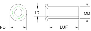
ID - Inside Diameter
Eyelet inside diameter should be 0.003"-0.020" greater than the component lead diameter.
OD - Outside Diameter
The clearance hole in the circuit board should be 0.001" to 0.005" greater than the outside diameter.
LUF - Length Under Flange
The length of the flange should be 0.020" - 0.035" greater than the thickness of the circuit board.
FD - Flange Diameter
The flange diameter should be small enough to prevent interference with adjacent pads or circuits.
The base metal is 1 oz copper with chemical etchant which allows for high bond strength to the PCB which will be repaired. The dimensions of the standard frames are 60 x 40 mm. The coating is on the PCB side is a shiny tin coating.
The film is a low stress epoxy film adhesive with a Tg at –60ºC. This minimizes the thermal stress on bonded parts during thermal cycling or shock testing from –55 to 150ºC. It is a clear 1mil (0.0254mm) in thickness nearly clear material. It has a shelf life 6 months minimum and is date-coded on the circuit frame to which it is bonded.
| Frame Size: | 57 x 38 mm (2.25" x 1.50") |
| Material: | Copper foil 0.036 mm (0.0014")-backside micro-etched for enhanced adhesion |
| Adhesive Backing: | Phenolic film adhesive 0.0254 mm (0.001") thick. |
| Electrical Resistivity: | Greater than 1014 ohm-cm |
| Dieletric Strength : | 750 Volts/mil |
| Glass Transition Temperature: | -60º C |
| Device push off strength: | Greater than 2,000psi, or 13.8N/mm2 |
| Peel Strength: | Greater than 9lbs/in (1.61 kg/cm) post cure to FR-4 |
| Hardness: | 65 Type A |
| Cured density: | 1.2 gm/cc |
| Thermal Conductivity: | 1.2 BUT-in/hr-ft2-ºF |
| Linear Thermal Expansion: | 110 ppm/ºC |
| Max Continuous Oper Temp: | 150ºC |
| Bonding Time: | 15 seconds |
| Bonding Temperature: | 200ºC |
| RoHS compliance: | YES |
| Shelf Life: | 6 months min. Circuit Frames are laser engraved with the expiration date. |

BEST can help you become more proficient at PCB repairs by offering a wide variety of tools to reduce the amount of time spent trimming circuit frames. Choose from a large variety of our different pads, traces, contact fingers and land patterns... or let us make a specialized version for you! We can turn these specialized patterns around for you quickly-as they are manufactured in house!
 Because BEST PCB repair kits are designed by artisans who repair circuit boards for a living the right tools have been included in our PCB repair kit.
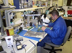
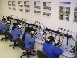
BEST Inc. PCB repair artisans have been involved in board level repairs for a combined 60 plus years. In addition, several BEST Inc staff members have been teaching and contributing to the procedures found in the IPC "7721 Repair and Modification of Printed Boards and Assemblies". This combined real life experience is captured through a series of "how to" slides which will guide you through the actual repair procedures. These instructions provide advanced repair technicians some "tricks of the trade" which are key when performing PCB repairs. Click here to look at these "how to" slides.


