

Call us Now! 1-847-797-9250
BEST soldering geeks enable electronics companies to be more effective through professional instruction, tools and taking secondary assembly projects off your plate


BEST soldering geeks enable electronics companies to be more effective through professional instruction, tools and taking secondary assembly projects off your plate
Develop Process Develop Profile Part Removal Site Preparation Placement Reflow Inspection
After removal of the BGA from the PCB the removal site must be dressed or prepared for the attachment of the replacement BGA. If the balls are eutectic alloy soldered to both the part and the PCB, some of the ball solder material will remain on the PCB after BGA removal. The remaining solder will be nonuniform in both composition and volume. The volume varies due to how the molten solder separates between the ball and the BGA pad surface. This operation entails removing all the solder balls and removing all of the solder residue. Only then can the site be dressed.
The dressing of the pads can be done by one of several methods. The methods for remnant solder removal includes solder wick or solder vacuum techniques. The solder vacuum process has less chance of damaging the pads while being somewhat slow. Some tools can be programmed for high volume BGA rework to remove solder via non contact extraction. The solder wicking technique, while faster, can lead to lifted pads or otherwise damaged solder mask areas if not done using the proper care/technique with the right size of wick.
After solder removal from the pads of the BGA site cleaning is performed. Cleaning processes and materials would follow those used in the initial assembly of the product.
Solder must be selectively applied to the BGA site pads in order to attach the solder balls of the BGA to the PCB. Solder paste is preferred as it provides a "tacking" functionality for the device being placed. In addition, it provides compensation for height differentials while overcoming warpage of the PCB or the component. Generally speaking it provides for a wider process window. Numerous studies have also concluded that the application of solder paste in BGA rework is critical in obtaining a highly reliable product. There are several methods which can be used to apply solder paste selectively to the prepared rework location.
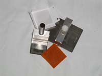
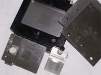
 Various types of stencils
There are numerous methods for selectively applying solder paste to the BGA rework pad locations. The most common stenciling methods include the use of metal stencils, flexible removable stencils as well as stay in place stencils. Each of these methods has distinct advantages over the other and is a function of lead time requirements, cost, operator skill level as well as other factors.
 Mini Metal Stencils Miniature metal stencils for depositing solder paste selectively on BGA pad locations have been in use for decades. Metal stencils for selective (a particular device, not the entire PCB) solder paste deposition have been in use almost as long. One of the greatest yield detractors in the SMT manufacturing process is the solder paste application process and the same holds true for the solder paste application process for rework. The process steps for using a component specific stencil for selective solder paste deposition for rework and a full PCB stencil for the original SMT manufacturing are almost identical. The major difference between the original stencil printing process and the selective solder paste printing process used for rework is the amount of process control. During the original solder paste stenciling process there are machine controls for the squeegee speed and pressure, snap-off distance, removal of the stencil from the board, and in some cases stencil alignment. The selective solder paste stenciling process is very dependent on the skill level of the technician to manually control these same variables. The metal stencil printing process begins with the stencil being aligned with the land patterns on the PCB, then the stencil must be held in place in a manner that ensures intimate contact with the PCB. Next, a squeegee is used to roll a bead of solder paste across and down through the apertures of the stencil. Finally, the stencil is lifted from the PCB surface resulting in finely defined solder paste deposits. If the stencil printing operation runs perfectly, the cycle time is very fast. Cleaning the stencil is a critical process step to ensure the stencil will provide acceptable results on the next BGA to be reworked. One variation on the metal stencil process is to print the solder paste directly onto the solder balls instead of the
BGA lands on the PCB. This method provides the advantage of printing solder paste where placing a stencil on the board would be impossible due to space considerations.
A robust easier to get right process for deposition of solder paste is the use of flexible solder paste stencils. These stencils are laser cut from a polymer film with a residue-free adhesive backing that allows for easy removal. The first step to using the flexible stencil is to remove the release liner to expose the adhesive backing. The stencil must then be manually aligned with the land patterns on the PCB and firmly pressed down in place on the PCB surface. A squeegee is then used to roll a bead of solder paste across and down through the apertures of the stencil. The stencil is then carefully removed from the PCB surface. There is no cleaning step as the stencil is disposable

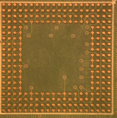
An alternative method of stenciling solder paste on the PCB is to use a stencil that remains in place on the site location and becomes an integral component of the PCB. The stencil material is a polyimide film with a high temperature adhesive covered with a paper backing. This material combination has been used on PCBs for many years in the form of bar code labels and Kapton(TM) tape. Like the removable stencil, the -permanent stencil is laser cut and can be provided in a number of different configurations. When using the semi-permanent stencil, the paper backing material is removed exposing the high temperature adhesive. The stencil is then manually aligned with the land patterns on the PCB and pressed into place. Again a squeegee is used to roll a bead of solder paste across and down through the apertures of the stencil. At this point the paste application process is complete and the device is reflowed. The stencil is not removed from the PCB and therefore no stencil cleaning step is required
 The advantages of Stencilquik(TM) BGA rework stencils
The following comparison chart compares and contrasts the various BGA rework stenciling technologies:
Comparison of (3) Most Common BGA Rework Stenciling Technologies
| BGA Rework Stencil Techniques | StencilQuik™ Permanent Stencil | StikNPeel(TM) Flexible, Plastic, Polymer Mini-Stencil | Traditional Flat or Formed Metal Mini-Stencil |
| Total Cost for Use | Lowest | Moderate | Highest |
| Damaged Solder Mask Repairs Required | No | Yes | Yes |
| Stencil Cleaning Cost | None | Moderate | High |
| Stencil Material Cost | Lowest | Moderate | High |
| Equipment Impact | For larger pitch components the need for high end rework systems may be eliminated | None | None |
| Operator Skill Level Requirement | Low | Moderate | High |
| Insulation in between balls | Excellent-StencilQuik™ acts as insulator between balls 10X increase in surface resistance | Adequate if site prepared properly | Adequate if site prepared properly |
| Volume Consistency of Paste Deposition | Fair - Dependent on stencil/circuit board flatness and operator squeegee skills. | Good - Flexible polymer with adhesive sealed apertures ensures consistent volume. | Fair - Dependent on stencil/circuit board flatness and operator squeegee skills. |
| Circuit Board and/or Device Planarity Requirements | Circuit board and stencil must be very flat. | Non-dependent on circuit board or component flatness. | Circuit board and stencil must be very flat. |
| Print Registration Accuracy | Excellent | Very Good-squeegee pressure is key | Fair Stencil must be carefully taped to circuit board surface. |
| Risk of Component Damage | None | None | None |
| Component Site Access | Good - Component perimeter clearance .025" - .075" typical. | Good - Component perimeter clearance .025" - .075" typical. | Fair - Component perimeter clearance .075" - .150" typical. |
| Stencil Maintenance & Cleaning Requirements | NOT REQUIRED. Stencils are affixed to the circuit board underneath the BGA | None - Stencils are disposable after single or multi-use. |
Moderate - Flatness must be maintained and apertures well cleaned between uses. |