BGA Pad Repair
Gold Fingers | BGA Pads | Plated holes | Edges | Mask | Populated Boards | Pad and Traces
BGA Pad Repair/Rework Services
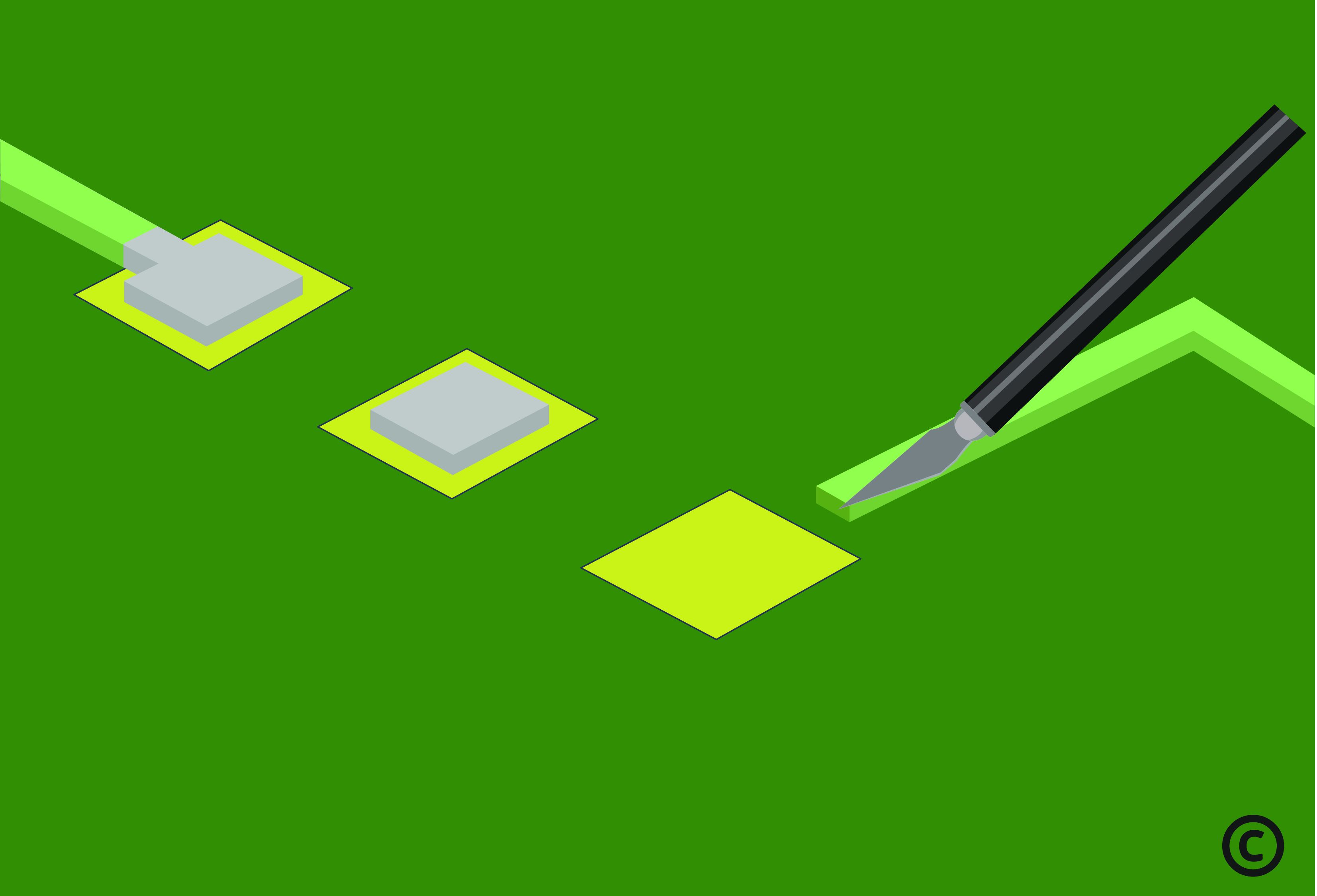
If BGA pads have been damaged due to improper part removal techniques, during reballing or mechanical "digging" into the circuit board during cleaning, then BEST can repair these damaged circuit patterns to as a "good as new" condition. If a critical part needs to have its pads repaired prior to reballing, then BEST can repair these BGA pads or vias. Finally, when an extra pad for testing or signal split off needs to be added to the PCB then the BEST BGA pad repair process can be used to add in a pad. No matter how small or big BEST technicians can do a high-quality job on your BGA pad repair.
BEST stocks many different kinds and styles of pads in order to facilitate a fast turnaround of the repair. We can even have the ability to make custom traces and pads in order to reduce the time and cost it takes to repair those boards. If there are numerous BGA pads requiring repair that of the same size or that or hooked into the same trace widths then BESTs’ BGA pad repair, design and manufacturing capability can design and fabricate a custom circuit frame in order to facilitate a faster turnaround and lower cost repair.
BEST repair technicians use the epoxy method as a standard matter of course when it comes to the repair of BGA pads. Using this method, the greatest pull strength (in fact our studies indicate a comparable pull strength to the original attachment) is achieved. The materials and processes used in our process have been qualified for use by the likes of Motorola, GE and Flextronics.
BEST technicians use a variety of different IPC repair techniques along with the "tricks of the trade" they have learned over many years when repairing. This is especially the case when a BGA pad repair which has an integral via is involved. In this case the via is connected to one or more of the internal layers. These internal layers need to be reconnected in many cases of BGA pad repair as the pad tens to “rip off” the connection to the via. This will enable them to accomplish a high-quality BGA pad repair where only a trained eye could discern that a repair had been performed.
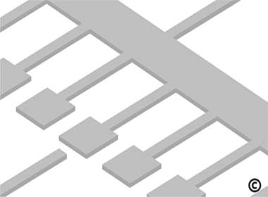
 BGA Pads Damaged
  BGA Pads Repaired
Procedure
1. Clean and inspect the repair area.

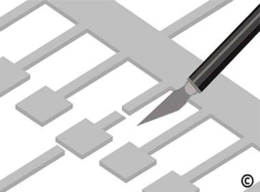
2. Remove the defective pad and a short length of the connecting circuit.
3. Using am exacto knife scrape off any epoxy residue, contamination or burned material from the board surface. In addition, scrape off any solder mask or coating from the connecting circuit.
4. Clean and inspect the repair area.
5. Apply a small amount of liquid flux to the connection area on the board surface and tin it with solder. Clean the area. The length of the overlapped butt solder connection should be a minimum of 2 times the circuit width.
6. The area for the new pad on the board surface should be flat with all of the roughness taken out.
7. Using a BEST circuit frame that includes a surface mount pad that most closely matches the pad to be replaced. If a special size or shape is needed it can be custom fabricated by BEST or a “make fit” can be created out of an existing circuit frame.
8. Cut out and trim the pad using an exacto knife. Cut the length to provide the maximum allowable circuit overlap for soldering.
9. Mix the epoxy per the manufacturer’s directions and apply a small amount to the surface where the new pad will be placed.
10. Place a piece of high temperature tape over the surface of the new pad. Place the new pad into position on the circuit board surface using the tape to help in alignment.

11. Cure the epoxy per the epoxy manufacturere’s specifications.
12. After the epoxy has cured remove the tape used for alignment. Carefully clean the area and inspect the new pad for assisting in alignment.

13. If the new pad has a connection to a trace, apply liquid flux to the lap solder joint connection area and solder the circuit from the new pad to the trace connection.
14. Mix epoxy per the manufacturer’s directions and coat the lap solder joint connections. Cure per the manufacturer's recommended instructions.

15. Apply liquid mask to match.
16. Clean and perform a Visual inspection per the IPC-A-610 requirements.
17. Test for electrical continuity.